参数资料
| 型号: | SC4524BSETRT |
| 厂商: | Semtech |
| 文件页数: | 13/18页 |
| 文件大小: | 0K |
| 描述: | IC REG BUCK 2A 8SOIC |
| 产品培训模块: | Power Supplies 101 |
| 标准包装: | 1 |
| 类型: | 降压(降压) |
| 输出数: | 1 |
| 输入电压: | 3 V ~ 18 V |
| PWM 型: | 电流模式 |
| 频率 - 开关: | 300kHz ~ 1.3MHz |
| 电流 - 输出: | 2A |
| 同步整流器: | 无 |
| 工作温度: | -40°C ~ 125°C |
| 安装类型: | 表面贴装 |
| 封装/外壳: | 8-SOIC(0.154",3.90mm Width)裸露焊盘 |
| 包装: | 标准包装 |
| 供应商设备封装: | 8-SOIC-EP |
| 产品目录页面: | 1358 (CN2011-ZH PDF) |
| 其它名称: | SC4524BSEDKR |
�� �
�
�SC4524B�
�Applications� Information� (Cont.)�
�CONTROLLER� AND� SCHOTTKY� DIODE�
�REF�
�+�
�CA�
�Rs�
�Io�
�Including� the� voltage� divider� (R� 4� and� R� 6� ),� the� control� to�
�feedback� transfer� function� is� found� and� plotted� in� Figure�
�8� as� the� converter� gain.�
�FB�
�-�
�EA�
�Vc�
�Vramp�
�PWM�
�MODULATOR�
�SW�
�L1�
�Vo�
�Since� the� converter� gain� has� only� one� dominant� pole� at�
�C5�
�R7�
�COMP�
�C8�
�Co�
�Resr�
�R4�
�R6�
�low� frequency,� a� simple� Type-2� compensation� network�
�is� sufficient� for� voltage� loop� compensation.� As� shown� in�
�Figure� 8,� the� voltage� compensator� has� a� low� frequency�
�integrator� pole,� a� zero� at� F� Z � ,� and� a� high� frequency� pole�
�at� F� P � .� The� integrator� is� used� to� boost� the� gain� at� low�
�frequency.� The� zero� is� introduced� to� compensate� the�
�excessive� phase� lag� at� the� loop� gain� crossover� due� to� the�
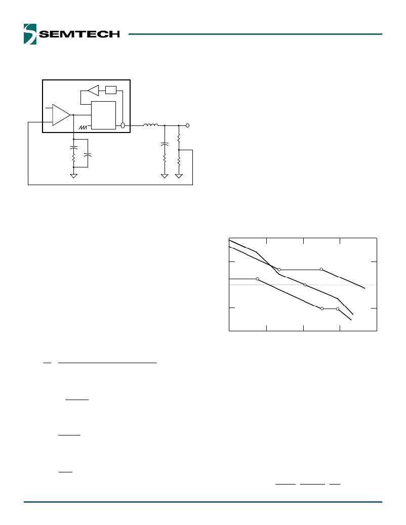
�The� block� =� =� diagram� log� ?� ?� ?� Figure� 7� ?� ?� shows� the� ?� ?� control� loops� of� a�
�?� ?� 20� ?� ?� log� G� R�
�A� A� C� C�
�?� � � V� FB� ?�
�V� V� O� O� ?� ?� ?�
�Figure7.Blockdiagramofcontrolloops�
�20� in� ?�
�?� ?� G� CA� R� π� π� F� F� C� C� C� O� O� CA�
�buck� converter� with� the� SC4524B.� The� inner� loop� (current�
�integrator� pole� (-90deg)� and� the� dominant� pole� (-90deg).�
�The� high� frequency� pole� nulls� the� ESR� zero� and� attenuates�
�high� frequency� noise.�
� � �
� � �
� � � .� .� 0� 0� 60� ?� 5� dB�
�loop)� consists� of� a� current� sensing� resistor� (R� s� =6. m� W� )�
�V� FB� ?� and� a� current� 20� ?� ?� log� ?� ?� ?� (CA)� with� gain� ?� ?� (G� CA� =28).� The� outer� ?� ?� 6� 6�
�?� ?� 3� .� 3� ?� ?� ?� =� =� 5� .� .� 9� 9� dB�
�?�
�A� A� C� C� =� =� ?� ?� 20� log�
�?� ?� loop� (voltage� loop)� consists� .� .� � � of� ?� ?� 0� error� π� π� amplifier� (EA),� ?� ?� 0�
�?� ?� 28� ?� ?� 6� 6�
�2� 2� ?� ?� 80� ?� ?� 0� 3� ?� ?� 22� a� 0�
�3� .� 3� ?� ?�
�28�
� 0�
�?�
�an�
�O� V� O� ?�
�MP�
�CO�
�EN�
� �
� 0� � .� 0� ?� 22� k�
� 0�
�SA�
� 5� .� 9�
�TO�
� � Since� 3� the� � =� =� current� FB� ?� loop� 3� 3� ?� is� =� =� internally� closed,� the� remaining�
�?�
�RG�
�20�
�R� R� ?� 22� ?� 0� ?� 6� V� 3� ?� ?� .� 3� ?� ?� ?� 5� .� .� 9� 3� 3� dB�
�?� 22� k� AIN�
�?� log� π� ?� ?� ?� 80� task� ?� for� the� 0� 0� loop� ?� ?� 0� ?�
�?� 0�
�2�
�?�
�.� .� 28� 0�
�28� compensation� is� to� design� the� voltage�
�7� 0� Fp�
�Fc�
�OP�
�R� S� 2� π� F� C� C� O�
�?� G� CA� compensator� (C� V� ,� R� ?� ,� and� C� ).�
�CO�
�NV� GA�
�ER�
� � � 8�
�TER�
�C� 5� =� =� 0� .� 45� nF�
�45� nF�
�5� 7� GA�
�C� 5�
�2� 2� π� π� ?� ?� 6� ?� ?� 0� � ?� ?� 22� .� .� � � ?� ?� 0� 3�
� 6� 0�
�22�
�?� log� ?� ?�
�For� a� converter� with� switching� frequency� =� 5� SW� .� ,� 9� dB�
� � � .� 0� ?�
�F� output�
�?�
�?�
� � � 3� ?� 22� ?� 0� ?� 6� 3� .� 3� ??�
�?� 6� .� � ?� 0� =�
�C� 8� =� � π� ?� 80� ?� 0� 3�
�?� 28� inductance� L� 2� ,� output� capacitance� C� =� and� pF�
�loading� R,� the�
�C� 8� O� =� 2� pF�
�control� (V� C� )� to� output� (V� O� )� transfer� function� in� Figure� 7� is�
�=� 0� .� 45� nF�
�=� 22� .� 3� k� V�
�G� PWM� (� � +� s� R� ESR� C� O� )�
�V� o� o� =�
�?� 0� 2� 3� pF�
�Figure� 8.� Bode� plots� for� voltage� loop� design�
�(8)�
�=�
�=� (� � +� s� /� ω� PWM� ()� � +� s� /� ω� ESR� Q� +� O� s� 2� 2� /� ω� 2� 2� )�
� � V� c� (� � +� s� /� ω� p� )� (� � +� s� /� ω� n� Q� +� s� /� ω� n� )�
�=� 0� .� 45� nF�
�3� This� transfer� function� has� a� finite� DC� gain� Therefore,� the� procedure� of� the� voltage� loop� design� for�
�6� ?� 0� ?� 22� .� � ?� 0�
�R� R�
� � �
� � �
� �
�G� PWM� 3� ≈� =� G� 2� pF� ,� ω� p� ≈� R� C� ,�
�ω� Z� Z� =� =� R�
�,� ,�
�G� CA� ?� R� S� R� ESR� C� O�
�00� /� ω� ?� 0� )� 3� ?� 22� .� � ?� 0�
�R� C� O�
�ESR�
�( )� Plot� the� converter� gain,� i.e.� control� to� feedback� transfer�
�amplifier�
�?� 3� 80� 0� 3� 22�
�PWM� modulator,� and� a� LC� filter.� 30� Fz1� Fp1�
� 5� .� 9�
�20�
�LO�
�O� IN�
�IN�
�3� 0� 3� -30�
�Fz� Fsw/2�
�?� 3�
�2� π� ?� 600� ?� 0� 3� ?� 22� .� � ?� 0� 3� -60�
�1K� 10K� 100K� 1M� 10M�
� 5� .� 9� given� by:� FREQUENCY� (Hz)�
�20�
�?�
�3�
�the� SC4524B� can� be� summarized� as:�
�G� PWM� ω� ω�
�2� 2�
�n� CA� S� O�
�an� ESR� zero� F� Z� at� CA� A� C�
� � G� PWM� (� � +� s� R� ESR� 7� 7� C� =� =� O� )� 0� �
�R�
�R� /� C� ω� O� p� )� (� � +� s� /� ω� n� Q� +� s� R� 2� g� ESR� ω� C� n� 2� O� )�
�C� C� 5� 5� =� =� π� F� R�
�a� dominant� 2� low-frequency� pole� F� P� at�
�2� π� F� Z� Z� � � R� 7� 7�
�ω� ≈�
�ω� Z� =�
�,�
� � ,�
�,�
�A� ?� R� S� C� p� =� R� C� O� � R� ESR� C� O�
�V� O�
�R� 4� =� R� 6� ?� ?� � ?�
�A� C� =� ?� 20� ?� log� ?� ?�
�?� FB� ?� ?�
�?� � � V� ?�
�A� C� =� ?� 20� ?� log� ?� ?�
�?�
�?� 28� ?� 6� .� � ?� 0�
�2� π� ?� 80� ?� 0� ?� 22� ?� 0�
�R� � �
� 0� 20� 20�
�R�
�,� ω� Z� =� g� m� ,�
�/� m�
� � �
�2� 2� π� π� F� F� P� P� � � R� R� 7� 7�
�and� double� poles� at� half� the� switching� frequency.�
�?� � .� 0� V� ?�
�function.�
�(2)� Select� the� open� loop� crossover� frequency,� F� C� ,� between�
� 0%� and� 20%� of� the� switching� frequency.� At� F� C� ,� find� the�
�required� compensator� gain,� A� C� .� In� typical� applications� with�
�ceramic� output� capacitors,� the� ESR� zero� is� neglected� and�
�the� required� compensator� gain� at� F� C� can� be� estimated� by�
�?� (9)�
�?� G� CA� R� S� 2� π� F� C� C� O� V� O� ?�
� � � 3�
�?� 3� 3�
�?� 6�
�?�
� � .� 0�
�3� .�
�相关PDF资料 |
PDF描述 |
|---|---|
| SC4524CSETRT | IC REG BUCK ADJ 2A 8SOIC |
| SC4524DSETRT | IC REG BUCK ADJ 2A 8SOIC |
| SC4524SETRT | IC REG BUCK 2A 8SOIC |
| SC4525ASETRT | IC REG BUCK 3A 8SOIC |
| SC4525CSETRT | IC REG BUCK ADJ 3A 8SOIC |
相关代理商/技术参数 |
参数描述 |
|---|---|
| SC4524C | 制造商:SEMTECH 制造商全称:Semtech Corporation 功能描述:28V 2A Step-Down Switching Regulator Wide input range: 3V to 28V |
| SC4524CSETRT | 功能描述:IC REG BUCK ADJ 2A 8SOIC RoHS:是 类别:集成电路 (IC) >> PMIC - 稳压器 - DC DC 开关稳压器 系列:- 标准包装:250 系列:- 类型:降压(降压) 输出类型:固定 输出数:1 输出电压:1.2V 输入电压:2.05 V ~ 6 V PWM 型:电压模式 频率 - 开关:2MHz 电流 - 输出:500mA 同步整流器:是 工作温度:-40°C ~ 85°C 安装类型:表面贴装 封装/外壳:6-UFDFN 包装:带卷 (TR) 供应商设备封装:6-SON(1.45x1) 产品目录页面:1032 (CN2011-ZH PDF) 其它名称:296-25628-2 |
| SC4524CSETRT-CUT TAPE | 制造商:SEMTECH 功能描述:SC4524 Series 28 V 2 A 2 MHz Step-Down Switching Regulator - SOIC-8 |
| SC4524D | 制造商:SEMTECH 制造商全称:Semtech Corporation 功能描述:18V 2A Step-Down Switching Regulator 2A Output Current |
| SC4524DSETRT | 功能描述:IC REG BUCK ADJ 2A 8SOIC RoHS:是 类别:集成电路 (IC) >> PMIC - 稳压器 - DC DC 开关稳压器 系列:- 标准包装:250 系列:- 类型:降压(降压) 输出类型:固定 输出数:1 输出电压:1.2V 输入电压:2.05 V ~ 6 V PWM 型:电压模式 频率 - 开关:2MHz 电流 - 输出:500mA 同步整流器:是 工作温度:-40°C ~ 85°C 安装类型:表面贴装 封装/外壳:6-UFDFN 包装:带卷 (TR) 供应商设备封装:6-SON(1.45x1) 产品目录页面:1032 (CN2011-ZH PDF) 其它名称:296-25628-2 |
发布紧急采购,3分钟左右您将得到回复。