- 您现在的位置:买卖IC网 > PDF目录45298 > SC515848CPV (FREESCALE SEMICONDUCTOR INC) 16-BIT, FLASH, 25 MHz, MICROCONTROLLER, PQFP112 PDF资料下载
参数资料
| 型号: | SC515848CPV |
| 厂商: | FREESCALE SEMICONDUCTOR INC |
| 元件分类: | 微控制器/微处理器 |
| 英文描述: | 16-BIT, FLASH, 25 MHz, MICROCONTROLLER, PQFP112 |
| 封装: | LQFP-112 |
| 文件页数: | 26/142页 |
| 文件大小: | 6464K |
| 代理商: | SC515848CPV |
第1页第2页第3页第4页第5页第6页第7页第8页第9页第10页第11页第12页第13页第14页第15页第16页第17页第18页第19页第20页第21页第22页第23页第24页第25页当前第26页第27页第28页第29页第30页第31页第32页第33页第34页第35页第36页第37页第38页第39页第40页第41页第42页第43页第44页第45页第46页第47页第48页第49页第50页第51页第52页第53页第54页第55页第56页第57页第58页第59页第60页第61页第62页第63页第64页第65页第66页第67页第68页第69页第70页第71页第72页第73页第74页第75页第76页第77页第78页第79页第80页第81页第82页第83页第84页第85页第86页第87页第88页第89页第90页第91页第92页第93页第94页第95页第96页第97页第98页第99页第100页第101页第102页第103页第104页第105页第106页第107页第108页第109页第110页第111页第112页第113页第114页第115页第116页第117页第118页第119页第120页第121页第122页第123页第124页第125页第126页第127页第128页第129页第130页第131页第132页第133页第134页第135页第136页第137页第138页第139页第140页第141页第142页
Device User Guide — 9S12DT128DGV2/D V02.15
121
Freescale Semiconductor
Clock Monitor Failure is asserted if the frequency of the incoming clock signal is below the Assert
Frequency fCMFA.
A.5.3 Phase Locked Loop
The oscillator provides the reference clock for the PLL. The PLLs Voltage Controlled Oscillator (VCO)
is also the system clock source in self clock mode.
A.5.3.1 XFC Component Selection
This section describes the selection of the XFC components to achieve a good filter characteristics.
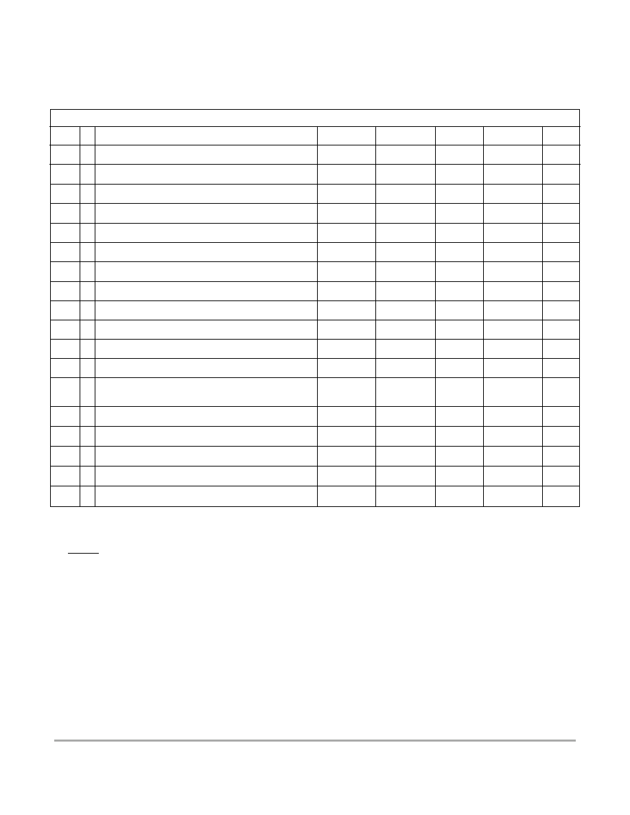
Table A-15 Oscillator Characteristics
Conditions are shown in (Table A-4) unless otherwise noted
Num C
Rating
Symbol
Min
Typ
Max
Unit
1a
C Crystal oscillator range (Colpitts)
fOSC
0.5
16
MHz
1b
C Crystal oscillator range (Pierce) 1
NOTES:
1. Depending on the crystal a damping series resistor might be necessary
fOSC
0.5
40
MHz
2
P Startup Current
iOSC
100
A
3
C Oscillator start-up time (Colpitts)
tUPOSC
82
2. fosc = 4MHz, C = 22pF.
1003
3. Maximum value is for extreme cases using high Q, low frequency crystals
ms
4
D Clock Quality check time-out
tCQOUT
0.45
2.5
s
5
P Clock Monitor Failure Assert Frequency
fCMFA
50
100
200
KHz
6
P External square wave input frequency 4
4. XCLKS =0 during reset
fEXT
0.5
50
MHz
7
D External square wave pulse width low
tEXTL
9.5
ns
8
D External square wave pulse width high
tEXTH
9.5
ns
9
D External square wave rise time
tEXTR
1
ns
10
D External square wave fall time
tEXTF
1
ns
11
D Input Capacitance (EXTAL, XTAL pins)
CIN
7
pF
12
C
DC Operating Bias in Colpitts Conguration on
EXTAL Pin
VDCBIAS
1.1
V
13
P EXTAL Pin Input High Voltage4
VIH,EXTAL
0.75*VDDPLL
V
T EXTAL Pin Input High Voltage4
VIH,EXTAL
VDDPLL + 0.3
V
14
P EXTAL Pin Input Low Voltage4
VIL,EXTAL
0.25*VDDPLL
V
T EXTAL Pin Input Low Voltage4
VIL,EXTAL
VSSPLL - 0.3
V
15
C EXTAL Pin Input Hysteresis4
VHYS,EXTAL
250
mV
相关PDF资料 |
PDF描述 |
|---|---|
| SC515847MFU | 16-BIT, FLASH, 25 MHz, MICROCONTROLLER, PQFP80 |
| MC9S12DJ128VPV | 16-BIT, FLASH, 25 MHz, MICROCONTROLLER, PQFP112 |
| MC9S12DJ128CFUE | 16-BIT, FLASH, 25 MHz, MICROCONTROLLER, PQFP80 |
| MC9S12DG128CPVE | 16-BIT, FLASH, 25 MHz, MICROCONTROLLER, PQFP112 |
| MC9S12DJ512VPVR2 | 16-BIT, FLASH, 25 MHz, MICROCONTROLLER, PQFP112 |
相关代理商/技术参数 |
参数描述 |
|---|---|
| SC515849 | 制造商:MOTOROLA 制造商全称:Motorola, Inc 功能描述:MC9S12DT128 Device User Guide V02.09 |
| SC516/WH | 制造商:CQR Security 功能描述:REED AND MAGNET HOUSING |
| SC51601FBR2 | 制造商:Motorola Inc 功能描述: |
| SC51613DWR2 | 制造商:Motorola Inc 功能描述: |
| SC516252CB | 制造商:Freescale Semiconductor 功能描述: |
发布紧急采购,3分钟左右您将得到回复。