- 您现在的位置:买卖IC网 > PDF目录11825 > SCC2691AC1D24,512 (NXP Semiconductors)IC UART SINGLE 24-SOL PDF资料下载
参数资料
| 型号: | SCC2691AC1D24,512 |
| 厂商: | NXP Semiconductors |
| 文件页数: | 20/25页 |
| 文件大小: | 0K |
| 描述: | IC UART SINGLE 24-SOL |
| 产品培训模块: | Stand-Alone UARTs |
| 标准包装: | 30 |
| 特点: | 故障启动位检测 |
| 通道数: | 1,UART |
| FIFO's: | 3 位 |
| 电源电压: | 5V |
| 带自动流量控制功能: | 是 |
| 带故障启动位检测功能: | 是 |
| 带CMOS: | 是 |
| 安装类型: | 表面贴装 |
| 封装/外壳: | 24-SOIC(0.295",7.50mm 宽) |
| 供应商设备封装: | 24-SO |
| 包装: | 管件 |
| 产品目录页面: | 828 (CN2011-ZH PDF) |
| 其它名称: | 568-1118-5 935002730512 SCC2691AC1D24 |
Philips Semiconductors
Product data sheet
SCC2691
Universal asynchronous receiver/transmitter (UART)
2006 Aug 04
4
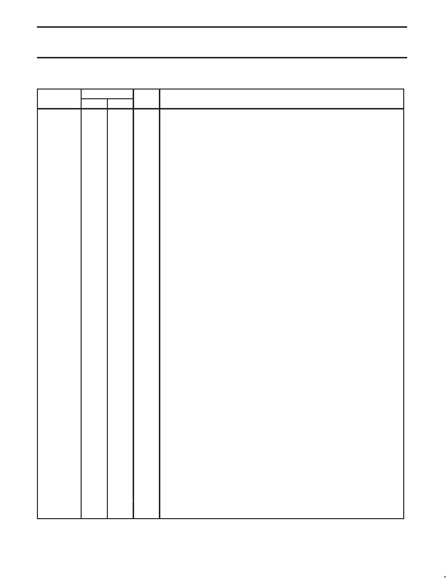
PIN DESCRIPTION
MNEMONIC
PIN NO.
TYPE
NAME AND FUNCTION
MNEMONIC
DIP
PLCC
TYPE
NAME AND FUNCTION
D0–D7
22–15
27, 25,
24,
22–18
I
Data Bus: Active-high 8-bit bidirectional 3-State data bus. Bit 0 is the LSB and bit 7 is the
MSB. All data, command, and status transfers between the CPU and the UART take place
over this bus. The direction of the transfer is controlled by the WRN and RDN inputs when
the CEN input is low. When the CEN input is high, the data bus is in the 3-State condition.
CEN
14
17
I
Chip Enable: Active-low input. When low, data transfers between the CPU and the UART
are enabled on D0–D7 as controlled by the WRN, RDN and A0–A2 inputs. When CEN is
high, the UART is effectively isolated from the data bus and D0–D7 are placed in the 3-State
condition.
WRN
23
28
I
Write Strobe: Active-low input. A low on this pin while CEN is low causes the contents of
the data bus to be transferred to the register selected by A0–A2. The transfer occurs on the
trailing (rising) edge of the signal.
RDN
1
2
I
Read Strobe: Active-low input. A low on this pin while CEN is low causes the contents of
the register selected by A0–A2 to be placed on the data bus. The read cycle begins on the
leading (falling) edge of RDN.
A0–A2
8–6
11–9
I
Address Inputs: Active-high address inputs to select the UART registers for read/write
operations.
RESET
11
14
I
Reset: Master reset. A high on this pin clears the status register (SR), the interrupt mask
register (IMR), and the interrupt status register (ISR), sets the mode register pointer to MR1,
and places the receiver and transmitter in the inactive state causing the TxD output to go to
the marking (high) state. Clears Test modes.
INTRN
13
16
O
Interrupt Request: This active-low output is asserted upon occurrence of one or more of
seven maskable interrupting conditions. The CPU can read the interrupt status register to
determine the interrupting condition(s). This open-drain output requires a pull-up resistor.
X1/CLK
9
12
I
Crystal 1: Crystal connection or an external clock input. A crystal of a clock the appropriate
frequency (nominally 3.6864 MHz) must be supplied at all times. For crystal connections see
Figure 7, Clock Timing.
X2
10
13
I
Crystal 2: Crystal connection. See Figure 7. If a crystal is not used it is best to keep this pin
not connected although it is permissible to ground it.
RxD
2
3
I
Receiver Serial Data Input: The least significant bit is received first. If external receiver
clock is specified, this input is sampled on the rising edge of the clock.
TxD
3
4
O
Transmitter Serial Data Output: The least significant bit is transmitted first. This output is
held in the marking (high) condition when the transmitter is idle or disabled and when the
UART is operating in local loopback mode. If external transmitter is specified, the data is
shifted on the falling edge of the transmitter clock.
MPO
4
5
O
Multi-Purpose Output: One of the following functions can be selected for this output pin by
programming the auxiliary control register:
RTSN – Request to send active-low output. This output is asserted and negated via the
command register. By appropriate programming of the mode registers, RTSN can be pro-
grammed to be automatically reset after the character in the transmitter is completely shifted
or when the receiver FIFO and shift register are full.
C/TO – The counter/timer output.
TxC1X – The 1X clock for the transmitter.
TxC16X – The 16X clock for the transmitter.
RxC1X – The 1X clock for the receiver.
RxC16X – The 16X clock for the receiver.
TxRDY – The transmitter holding register empty signal. Active-low output. (Open drain)
RxRDY/FFULL – The receiver FIFO not empty/full signal. Active-low output. (Open drain)
MPI
5
6
I
Multi-Purpose Input: This pin can serve as an input for one of the following functions:
GPI – General purpose input. The current state of the pin can be determined by reading the
ISR.
CTSN – Clear-to-send active-low input.
CTCLK – Counter/timer external clock input.
RTCLK – Receiver and/or transmitter external clock input. This may be a 1X or 16X clock as
programmed by CSR[3:0] or CSR[7:4].
Pin has an internal VCC pull-up device supplying 1 to 4 mA of current.
VCC
24
1
I
Power Supply: +5V supply input.
GND
12
15
I
Ground
相关PDF资料 |
PDF描述 |
|---|---|
| MS27484T18A35P | CONN PLUG 66POS STRAIGHT W/PINS |
| MS3100E24-28S | CONN RCPT 24POS WALL MNT W/SCKT |
| SC16C750BIBS,151 | IC UART SINGLE W/FIFO 32-HVQFN |
| MS27484T14A35S | CONN PLUG 37POS STRAIGHT W/SCKT |
| SC16C750BIA44,518 | IC UART SINGLE W/FIFO 44-PLCC |
相关代理商/技术参数 |
参数描述 |
|---|---|
| SCC2691AC1N24 | 制造商:NXP Semiconductors 功能描述:IC UART, ASYNCHRONOUS, DIP 24 PIN 制造商:NXP Semiconductors 功能描述:IC UART 2691 DIP24 制造商:NXP Semiconductors 功能描述:IC, UART, 2691, DIP24 制造商:NXP Semiconductors 功能描述:IC, SGL UART, FIFO, 115KBAUD, 5.5V DIP24; No. of Channels:1; Supply Voltage Min:4.5V; Supply Voltage Max:5.5V; Digital IC Case Style:DIP; No. of Pins:24; Operating Temperature Min:0C; Operating Temperature Max:70C ;RoHS Compliant: Yes 制造商:Philips 功能描述:UART 1-CH 5V 24-Pin PDIP 制造商:NXP Semiconductors 功能描述:UART 1-CH 5V 24-Pin PDIP |
| SCC2691AC1N24,129 | 功能描述:UART 接口集成电路 5V INDSTRL UART 1 C RoHS:否 制造商:Texas Instruments 通道数量:2 数据速率:3 Mbps 电源电压-最大:3.6 V 电源电压-最小:2.7 V 电源电流:20 mA 最大工作温度:+ 85 C 最小工作温度:- 40 C 封装 / 箱体:LQFP-48 封装:Reel |
| SCC2691AC1N24,602 | 功能描述:UART 接口集成电路 1CH. 5V IND. UART RoHS:否 制造商:Texas Instruments 通道数量:2 数据速率:3 Mbps 电源电压-最大:3.6 V 电源电压-最小:2.7 V 电源电流:20 mA 最大工作温度:+ 85 C 最小工作温度:- 40 C 封装 / 箱体:LQFP-48 封装:Reel |
| SCC2691AC1N24 | 制造商:NXP Semiconductors 功能描述:IC UART 2691 DIP24 |
| SCC2691AC1N24129 | 制造商:NXP Semiconductors 功能描述:IC SGL UART FIFO 115KBAUD 5.5V DIP24 |
发布紧急采购,3分钟左右您将得到回复。