- 您现在的位置:买卖IC网 > PDF目录11825 > SCC2691AC1D24,512 (NXP Semiconductors)IC UART SINGLE 24-SOL PDF资料下载
参数资料
| 型号: | SCC2691AC1D24,512 |
| 厂商: | NXP Semiconductors |
| 文件页数: | 23/25页 |
| 文件大小: | 0K |
| 描述: | IC UART SINGLE 24-SOL |
| 产品培训模块: | Stand-Alone UARTs |
| 标准包装: | 30 |
| 特点: | 故障启动位检测 |
| 通道数: | 1,UART |
| FIFO's: | 3 位 |
| 电源电压: | 5V |
| 带自动流量控制功能: | 是 |
| 带故障启动位检测功能: | 是 |
| 带CMOS: | 是 |
| 安装类型: | 表面贴装 |
| 封装/外壳: | 24-SOIC(0.295",7.50mm 宽) |
| 供应商设备封装: | 24-SO |
| 包装: | 管件 |
| 产品目录页面: | 828 (CN2011-ZH PDF) |
| 其它名称: | 568-1118-5 935002730512 SCC2691AC1D24 |
Philips Semiconductors
Product data sheet
SCC2691
Universal asynchronous receiver/transmitter (UART)
2006 Aug 04
7
BLOCK DIAGRAM
As shown in the block diagram, the UART consists of: data bus buffer,
interrupt control, operation control, timing, receiver and transmitter.
Data Bus Buffer
The data bus buffer provides the interface between the external and
internal data busses. It is controlled by the operation control block to
allow read and write operations to take place between the controlling
CPU and UART.
Interrupt Control
A single interrupt output (INTRN) is provided which may be asserted
upon occurrence of any of the following internal events:
– Transmit holding register ready
– Transmit shift register empty
– Receive holding register ready or FIFO full
– Change in break received status
– Counter reached terminal count
– Change in MPI input
– Assertion of MPI input
Associated with the interrupt system are the interrupt mask register
(IMR) and the interrupt status register (ISR). The IMR can be
programmed to select only certain of the above conditions to cause
INTRN to be asserted. The ISR can be read by the CPU to
determine all currently active interrupting conditions. However, the
bits of the ISR are not masked by the IMR.
Operation Control
The operation control logic receives operation commands from the
CPU and generates appropriate signals to internal sections to
control device operation. It contains address decoding and read and
write circuits to permit communications with the microprocessor via
the data bus buffer. The functions performed by the CPU read and
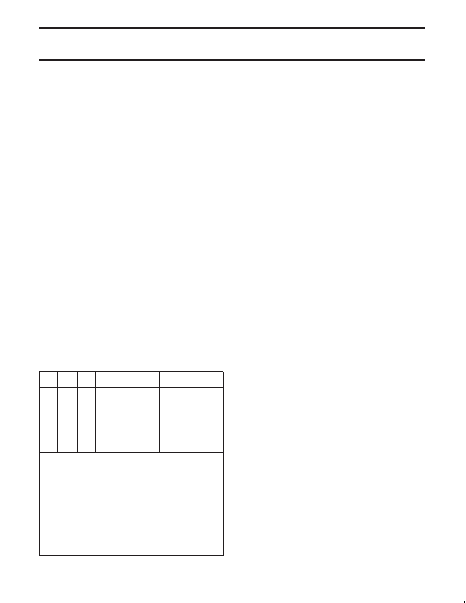
write operations are shown in Table 1.
Table 1.
Register Addressing
A2
A1
A0
READ
(RDN = 0)
WRITE
(WRN = 0)
0
MR1, MR2
0
1
SR
CSR
0
1
0
BRG Test
CR
0
1
RHR
THR
1
0
1X/16X Test
ACR
1
0
1
ISR
IMR
1
0
CTU
CTUR
1
CTL
CTLR
NOTE;
*Reserved registers should never be read during operation since
they are reserved for internal diagnostics.
ACR = Auxiliary control register
CR = Command register
CSR = Clock select register
CTL = Counter/timer lower output register
CTLR = Counter/timer lower preset register
CTU = Counter/timer upper output register
CTUR = Counter/timer upper preset register
MR = Mode register A
SR = Status register
THR = Tx holding register
* See Table 6 for BRG Test frequencies in this data sheet, and
“Extended baud rates for SCN2681, SCN68681, SCC2691,
SCC2692, SCC68681 and SCC2698B” Philips Semiconductors ICs
for Data Communications, IC-19, 1994.
Mode registers 1 and 2 are accessed via an auxiliary pointer. The
pointer is set to MR1 by RESET or by issuing a reset pointer
command via the command register. Any read or write of the mode
register while the pointer is at MR1 switches the pointer to MR2. the
pointer then remains at MR2 so that subsequent accesses are to
MR2, unless the pointer is reset to MR1 as described above.
Timing Circuits
The timing block consists of a crystal oscillator, a baud rate
generator, a programmable 16-bit counter/timer, and two clock
selectors.
The crystal oscillator operates directly from a 3.6864MHz crystal
connected across the X1/ CLK and X2 inputs with a minimum of
external components. If an external clock of the appropriate
frequency is available, it may be connected to X1/CLK. If an external
clock is used instead of a crystal, X1/CLK is driven using a
configuration similar to the one in Figure 7. In this case, the input
high-voltage must be capable of attaining the voltage specified in the
DC Electrical Characteristics. The clock serves as the basic timing
reference for the baud rate generator (BRG), the counter/timer, and
other internal circuits. A clock frequency, within the limits specified in
the electrical specifications, must be supplied if the internal BRG is
not used.
The baud rate generator operates from the oscillator or external
clock input and is capable of generating 18 commonly used data
communications baud rates ranging from 50 to 38.4K baud. Thirteen
of these are available simultaneously for use by the receiver and
transmitter. Eight are fixed, and one of two sets of five can be
selected by programming ACR[7]. The clock outputs from the BRG
are at 16X the actual baud rate. The counter/timer can be used as a
timer to produce a 16X clock for any other baud rate by counting
down the crystal clock or an external clock. The clock selectors
allow the independent selection by the receiver and transmitter of
any of these baud rates or an external timing signal.
Counter/Timer (C/T)
The C/T operation is programmed by ACR[6:4]. One of eight timing
sources can be used as the input to the C/T. The output of the C/T is
available to the clock selectors and can be programmed by
ACR[2:0} to be output on the MPO pin.
In the timer mode, the C/T generates a square wave whose period is
twice the number of clock periods loaded into the C/T upper and
lower registers. The counter ready bit in the ISR is set once each
cycle of the square wave. If the value in CTUR or CTLR is changed,
the current half-period will not be affected, but subsequent
half-periods will be affected. In this mode the C/T runs continuously
and does not recognize the stop counter command (the command
only resets the counter ready bit in the ISR). Receipt of a start C/T
command causes the counter to terminate the current timing cycle
and to begin a new cycle using the values in CTUR and CTLR.
In the counter mode, the C/T counts down the number of pulses
loaded into CTUR and CTLR. Counting begins upon receipt of a
start C/T command. Upon reaching terminal count, the counter
ready bit in the ISR is set. The counter continues counting past the
terminal count until stopped by the CPU. If MPO is programmed to
be the output of the C/T, the output remains high until terminal count
is reached, at which time it goes low. The output returns to the high
state and the counter ready bit is cleared when the counter is
stopped by a stop counter command. the CPU may change the
相关PDF资料 |
PDF描述 |
|---|---|
| MS27484T18A35P | CONN PLUG 66POS STRAIGHT W/PINS |
| MS3100E24-28S | CONN RCPT 24POS WALL MNT W/SCKT |
| SC16C750BIBS,151 | IC UART SINGLE W/FIFO 32-HVQFN |
| MS27484T14A35S | CONN PLUG 37POS STRAIGHT W/SCKT |
| SC16C750BIA44,518 | IC UART SINGLE W/FIFO 44-PLCC |
相关代理商/技术参数 |
参数描述 |
|---|---|
| SCC2691AC1N24 | 制造商:NXP Semiconductors 功能描述:IC UART, ASYNCHRONOUS, DIP 24 PIN 制造商:NXP Semiconductors 功能描述:IC UART 2691 DIP24 制造商:NXP Semiconductors 功能描述:IC, UART, 2691, DIP24 制造商:NXP Semiconductors 功能描述:IC, SGL UART, FIFO, 115KBAUD, 5.5V DIP24; No. of Channels:1; Supply Voltage Min:4.5V; Supply Voltage Max:5.5V; Digital IC Case Style:DIP; No. of Pins:24; Operating Temperature Min:0C; Operating Temperature Max:70C ;RoHS Compliant: Yes 制造商:Philips 功能描述:UART 1-CH 5V 24-Pin PDIP 制造商:NXP Semiconductors 功能描述:UART 1-CH 5V 24-Pin PDIP |
| SCC2691AC1N24,129 | 功能描述:UART 接口集成电路 5V INDSTRL UART 1 C RoHS:否 制造商:Texas Instruments 通道数量:2 数据速率:3 Mbps 电源电压-最大:3.6 V 电源电压-最小:2.7 V 电源电流:20 mA 最大工作温度:+ 85 C 最小工作温度:- 40 C 封装 / 箱体:LQFP-48 封装:Reel |
| SCC2691AC1N24,602 | 功能描述:UART 接口集成电路 1CH. 5V IND. UART RoHS:否 制造商:Texas Instruments 通道数量:2 数据速率:3 Mbps 电源电压-最大:3.6 V 电源电压-最小:2.7 V 电源电流:20 mA 最大工作温度:+ 85 C 最小工作温度:- 40 C 封装 / 箱体:LQFP-48 封装:Reel |
| SCC2691AC1N24 | 制造商:NXP Semiconductors 功能描述:IC UART 2691 DIP24 |
| SCC2691AC1N24129 | 制造商:NXP Semiconductors 功能描述:IC SGL UART FIFO 115KBAUD 5.5V DIP24 |
发布紧急采购,3分钟左右您将得到回复。