- 您现在的位置:买卖IC网 > PDF目录11824 > SCC68681C1A44,518 (NXP Semiconductors)IC DUART 44PLCC PDF资料下载
参数资料
| 型号: | SCC68681C1A44,518 |
| 厂商: | NXP Semiconductors |
| 文件页数: | 29/29页 |
| 文件大小: | 0K |
| 描述: | IC DUART 44PLCC |
| 标准包装: | 500 |
| 特点: | 故障启动位检测 |
| 通道数: | 2,DUART |
| FIFO's: | 3 位 |
| 电源电压: | 5V |
| 带自动流量控制功能: | 是 |
| 带故障启动位检测功能: | 是 |
| 带CMOS: | 是 |
| 安装类型: | 表面贴装 |
| 封装/外壳: | 44-LCC(J 形引线) |
| 供应商设备封装: | 44-PLCC |
| 包装: | 带卷 (TR) |
| 其它名称: | 935274497518 SCC68681C1A44-T SCC68681C1A44-T-ND |
第1页第2页第3页第4页第5页第6页第7页第8页第9页第10页第11页第12页第13页第14页第15页第16页第17页第18页第19页第20页第21页第22页第23页第24页第25页第26页第27页第28页当前第29页
Philips Semiconductors
Product data
SCC68681
Dual asynchronous receiver/transmitter (DUART)
2004 Apr 06
9
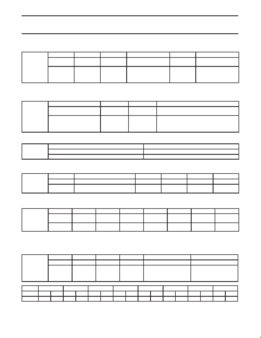
Table 2.
Register Bit Formats
BIT 7
BIT 6
BIT 5
BIT 4
BIT 3
BIT 2
BIT 1
BIT 0
MR1A
RxRTS
CONTROL
RxINT
SELECT
ERROR
MODE*
PARITY MODE
PARITY
TYPE
BITS PER
CHARACTER
MR1A
MR1B
0 = No
1 = Yes
0 = RxRDY
1 = FFULL
0 = Char
1 = Block
00 = With Parity
01 = Force Parity
10 = No Parity
11 = Multidrop Mode**
0 = Even
1 = Odd
00 = 5
01 = 6
10 = 7
11 = 8
NOTE:
* In block error mode, block error conditions must be cleared by using the error reset command (command 4x) or a receiver reset.
** Please see Receiver Reset note on page 19.
BIT 7
BIT 6
BIT 5
BIT 4
BIT 3
BIT 2
BIT 1
BIT 0
MR2A
CHANNEL MODE
TxRTS
CONTROL
CTS
ENABLE Tx
STOP BIT LENGTH*
MR2A
MR2B
00 = Normal
01 = Auto-Echo
10 = Local loop
11 = Remote loop
0 = No
1 = Yes
0 = No
1 = Yes
0 = 0.563
4 = 0.813
8 = 1.563
C = 1.813
1 = 0.625
5 = 0.875
9 = 1.625
D = 1.875
2 = 0.688
6 = 0.938
A = 1.688
E = 1.938
3 = 0.750
7 = 1.000
B = 1.750
F = 2.000
NOTE:
*Add 0.5 to values shown for 0 - 7 if channel is programmed for 5 bits/char.
CSRA
BIT 7
BIT 6
BIT 5
BIT 4
BIT 3
BIT 2
BIT 1
BIT 0
CSRA
CSRB
RECEIVER CLOCK SELECT
TRANSMITTER CLOCK SELECT
CSRB
See Text
NOTE:
* See Table 6 for BRG Test frequencies in this data sheet, and
“Extended baud rates for SCN2681, SCN68681, SCC2691, SCC2692,
SCC68681 and SCC2698B” in application notes elsewhere in this publication
BIT 7
BIT 6
BIT 5
BIT 4
BIT 3
BIT 2
BIT 1
BIT 0
CRA
CRB
MISCELLANEOUS COMMANDS
DISABLE Tx
ENABLE Tx
DISABLE Rx
ENABLE Rx
CRB
Not used –
must be 0
See Text
0 = No
1 = Yes
0 = No
1 = Yes
0 = No
1 = Yes
0 = No
1 = Yes
NOTE:
*Access to the upper four bits of the command register should be separated by three (3) edges of the X1 clock. A disabled transmitter cannot
be loaded. For Rx and Tx performing a Disable and Enable at the same time results in Disable.
BIT 7
BIT 6
BIT 5
BIT 4
BIT 3
BIT 2
BIT 1
BIT 0
SRA
SRB
RECEIVED
BREAK*
FRAMING
ERROR*
PARITY
ERROR*
OVERRUN
ERROR
TxEMT
TxRDY
FFULL
RxRDY
SRB
0 = No
1 = Yes
0 = No
1 = Yes
0 = No
1 = Yes
0 = No
1 = Yes
0 = No
1 = Yes
0 = No
1 = Yes
0 = No
1 = Yes
0 = No
1 = Yes
NOTE:
*These status bits are appended to the corresponding data character in the receive FIFO. A read of the status provides these bits (7:5) from the
top of the FIFO together with bits (4:0). These bits are cleared by a ‘reset error status’ command. In character mode they are discarded when
the corresponding data character is read from the FIFO. In block error mode, block error conditions must be cleared by using the error reset
command (command 4x) or a receiver reset.
BIT 7
BIT 6
BIT 5
BIT 4
BIT 3
BIT 2
BIT 1
BIT 0
OP7
OP6
OP5
OP4
OP3
OP2
OPCR
0 = OPR[7]
1 = TxRDYB
0 = OPR[6]
1 = TxRDYA
0 = OPR[5]
1 = RxRDY/
FFULLB
0 = OPR[4]
1 = RxRDY/
FFULLA
00 = OPR[3]
01 = C/T OUTPUT
10 = TxCB(1
×)
11 = RxCB(1
×)
00 = OPR[2]
01 = TxCA(16
×)
10 = TxCA(1
×)
11 = RxCA(1
×)
OPR
BIT 7
BIT 6
BIT 5
BIT 4
BIT 3
BIT 2
BIT 1
BIT 0
OPR bit
0
1
0
1
0
1
0
1
0
1
0
1
0
1
0
1
OP pin
1
0
1
0
1
0
1
0
1
0
1
0
1
0
1
0
NOTE:
The level at the OP pin is the inverse of the bit in the OPR register.
相关PDF资料 |
PDF描述 |
|---|---|
| VE-BTN-IW-F3 | CONVERTER MOD DC/DC 18.5V 100W |
| VI-26J-IY | CONVERTER MOD DC/DC 36V 50W |
| MS27484E10B99P | CONN PLUG 7POS STRAIGHT W/PINS |
| VE-BTN-IW-F1 | CONVERTER MOD DC/DC 18.5V 100W |
| SC28L91A1A,512 | IC UART SINGLE W/FIFO 44-PLCC |
相关代理商/技术参数 |
参数描述 |
|---|---|
| SCC68681C1A44-T | 功能描述:UART 接口集成电路 RPLCMNT FOR SCN68681 RoHS:否 制造商:Texas Instruments 通道数量:2 数据速率:3 Mbps 电源电压-最大:3.6 V 电源电压-最小:2.7 V 电源电流:20 mA 最大工作温度:+ 85 C 最小工作温度:- 40 C 封装 / 箱体:LQFP-48 封装:Reel |
| SCC68681C1N40 | 制造商:PHILIPS 制造商全称:NXP Semiconductors 功能描述:Dual asynchronous receiver/transmitter |
| SCC68681C1N40,112 | 功能描述:UART 接口集成电路 2CH.UART RoHS:否 制造商:Texas Instruments 通道数量:2 数据速率:3 Mbps 电源电压-最大:3.6 V 电源电压-最小:2.7 V 电源电流:20 mA 最大工作温度:+ 85 C 最小工作温度:- 40 C 封装 / 箱体:LQFP-48 封装:Reel |
| SCC68681C1N40112 | 制造商:Rochester Electronics LLC 功能描述: 制造商:NXP 功能描述: 制造商:NXP Semiconductors 功能描述: |
| SCC68681E1A44 | 功能描述:UART 接口集成电路 RPLCMNT FOR SCN68681 RoHS:否 制造商:Texas Instruments 通道数量:2 数据速率:3 Mbps 电源电压-最大:3.6 V 电源电压-最小:2.7 V 电源电流:20 mA 最大工作温度:+ 85 C 最小工作温度:- 40 C 封装 / 箱体:LQFP-48 封装:Reel |
发布紧急采购,3分钟左右您将得到回复。