- 您现在的位置:买卖IC网 > PDF目录11823 > SCC68681E1A44,518 (NXP Semiconductors)IC DUART 44PLCC PDF资料下载
参数资料
| 型号: | SCC68681E1A44,518 |
| 厂商: | NXP Semiconductors |
| 文件页数: | 14/29页 |
| 文件大小: | 0K |
| 描述: | IC DUART 44PLCC |
| 标准包装: | 500 |
| 特点: | 故障启动位检测 |
| 通道数: | 2,DUART |
| FIFO's: | 3 位 |
| 电源电压: | 5V |
| 带自动流量控制功能: | 是 |
| 带故障启动位检测功能: | 是 |
| 带CMOS: | 是 |
| 安装类型: | 表面贴装 |
| 封装/外壳: | 44-LCC(J 形引线) |
| 供应商设备封装: | 44-PLCC |
| 包装: | 带卷 (TR) |
| 其它名称: | 935274496518 SCC68681E1A44-T SCC68681E1A44-T-ND |
第1页第2页第3页第4页第5页第6页第7页第8页第9页第10页第11页第12页第13页当前第14页第15页第16页第17页第18页第19页第20页第21页第22页第23页第24页第25页第26页第27页第28页第29页
Philips Semiconductors
Product data
SCC68681
Dual asynchronous receiver/transmitter (DUART)
2004 Apr 06
21
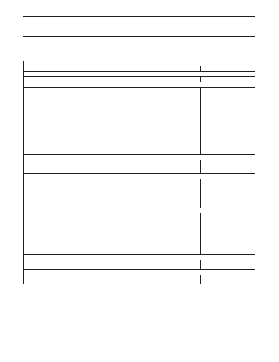
AC CHARACTERISTICS 1, 2, 3, 4
Tamb = –40 °C to +85 °C; VCC = 5.0 V ± 10%
SYMBOL
PARAMETER
LIMITS
UNIT
SYMBOL
PARAMETER
Min
Typ3
Max
UNIT
Reset Timing (See Figure 3)
tRES
RESETN pulse width
200
ns
Bus Timing (See Figures 4, 5, 6)
tAS
A1–A4 setup time to CSN LOW
10
–
ns
tAH
A1–A4 hold time from CSN LOW
100
–
ns
tRWS
RWN setup time to CSN HIGH
0
–
ns
tRWH
RWN hold time to CSN HIGH
0
–
ns
tCSW
CSN HIGH pulse width
90
–
ns
tCSD5
CSN or IACKN HIGH from DTACKN LOW
20
–
ns
tDD
Data valid from CSN or IACKN LOW
–
175
ns
tDF
Data bus floating from CSN or IACKN HIGH7
–
100
ns
tDS
Data setup time to CLK HIGH
100
–
ns
tDH
Data hold time from CSN HIGH
20
–
ns
tDAL
DTACKN LOW from read data valid
0
–
ns
tDCR
DTACKN LOW (read cycle) from CLK HIGH
–
125
ns
tDCW
DTACKN LOW (write cycle) from CLK HIGH
–
125
ns
tDAH
DTACKN HIGH from CSN or IACKN HIGH
–
100
ns
tDAT
DTACKN HIGH impedance from CSN or IACKN HIGH
–
125
ns
tCSC6
CSN or IACKN setup time to clock HIGH
90
–
ns
Port Timing (See Figure 7)
tPS
Port input setup time to CSN LOW
0
–
ns
tPH
Port input hold time from CSN HIGH
0
–
ns
tPD
Port output valid from CSN HIGH
–
400
ns
Interrupt Reset Timing (See Figure 9)
INTRN or OP3–OP7 when used as interrupts negated from:
Read RHR (RxRDY/FFULL interrupt)
–
300
ns
Write THR (TxRDY interrupt)
–
300
ns
tIR
Reset command (delta break interrupt)
–
300
ns
IR
Stop C/T command (counter interrupt)
–
300
ns
Read IPCR (input port change interrupt)
–
300
ns
Write IMR (clear of interrupt mask bit)
–
300
ns
Clock Timing (See Figure 8)
tCLK
X1/CLK HIGH or LOW time
100
–
ns
fCLK8
X1/CLK frequency
0
3.6864
4.0
MHz
tCTC
CTCLK HIGH or LOW time
100
–
ns
fCTC
CTCLK frequency
0
–
4.0
MHz
tRX
RxC HIGH or LOW time
220
–
ns
fRX
RxC frequency
(16
×)
0
–
2.0
MHz
RX
(1
×)
0
–
1.0
MHz
tTX
TxC HIGH or LOW time
220
–
ns
fTX
TxC frequency
(16
×)
0
–
2.0
MHz
TX
(1
×)
0
–
1.0
MHz
Transmitter Timing (See Figure 10)
tTXD
TxD output delay from TxC external clock input on IP pin
–
350
ns
tTCS
Output delay from TxC LOW at OP pin to TxD data output
–
150
ns
Receiver Timing (See Figure 11)
tRXS
RxD data setup time before RxC HIGH at external clock input on IP pin
240
–
ns
tRXH
RxD data hold time after RxC HIGH at external clock input on IP pin
200
–
ns
NOTES:
1. Parameters are valid over specified temperature range. See Ordering information table for applicable operating temperature and VCC supply
range.
2. All voltage measurements are referenced to ground (GND). For testing, all inputs except X1/CLK swing between 0.4 V and 2.4 V with
a transition time of 20 ns maximum. For X1/CLK this swing is between 0.4 V and 4.4 V. All time measurements are referenced at input
voltages of 0.8 V and 2.0 V as appropriate.
3. Typical values are at +25
°C, typical supply voltages, and typical processing parameters.
4. Test conditions for outputs: CL = 150 pF, except interrupt outputs. Test condition for interrupt outputs: CL = 50 pF, RL = 2.7 k to VCC.
5. This specification will impose maximum 68000 CPU CLK to 6MHz. Higher CPU CLK can be used if repeating bus reads are not performed.
Consecutive write operations to the same command register require at least three edges of the X1 clock between writes.
6. This specification imposes a lower bound on CSN and IACKN LOW, guaranteeing that it will be LOW for at least 1 CLK period. This
requirement is made on CSN only to insure assertion of DTACKN and not to guarantee operation of the part.
7. This spec is made only to insure that DTACKN is asserted with respect to the rising edge of the X1/CLK pin as shown in the timing diagram,
not to guarantee operation of the part. If setup time is violated, DTACKN may be asserted as shown, or may be asserted 1 clock cycle later.
8. Operation to 0 MHz is assured by design. Minimum test frequency is 2.0 MHz.
相关PDF资料 |
PDF描述 |
|---|---|
| SC28L91A1A,518 | IC UART SINGLE W/FIFO 44-PLCC |
| SCC68692E1A44,512 | IC DUART 44PLCC |
| SCC2691AE1A28,623 | IC UART SOT261-2 |
| VI-B4Z-IY | CONVERTER MOD DC/DC 2V 20W |
| VI-B4Z-IX | CONVERTER MOD DC/DC 2V 30W |
相关代理商/技术参数 |
参数描述 |
|---|---|
| SCC68681E1A44-S | 功能描述:UART 接口集成电路 RPLCMNT FOR SCN68681 RoHS:否 制造商:Texas Instruments 通道数量:2 数据速率:3 Mbps 电源电压-最大:3.6 V 电源电压-最小:2.7 V 电源电流:20 mA 最大工作温度:+ 85 C 最小工作温度:- 40 C 封装 / 箱体:LQFP-48 封装:Reel |
| SCC68681E1A44-T | 功能描述:UART 接口集成电路 RPLCMNT FOR SCN68681 RoHS:否 制造商:Texas Instruments 通道数量:2 数据速率:3 Mbps 电源电压-最大:3.6 V 电源电压-最小:2.7 V 电源电流:20 mA 最大工作温度:+ 85 C 最小工作温度:- 40 C 封装 / 箱体:LQFP-48 封装:Reel |
| SCC68681E1N40 | 功能描述:UART 接口集成电路 RPLCMNT FOR SCN68681 RoHS:否 制造商:Texas Instruments 通道数量:2 数据速率:3 Mbps 电源电压-最大:3.6 V 电源电压-最小:2.7 V 电源电流:20 mA 最大工作温度:+ 85 C 最小工作温度:- 40 C 封装 / 箱体:LQFP-48 封装:Reel |
| SCC68681E1N40,112 | 功能描述:UART 接口集成电路 RPLCMNT FOR SCN68681 RoHS:否 制造商:Texas Instruments 通道数量:2 数据速率:3 Mbps 电源电压-最大:3.6 V 电源电压-最小:2.7 V 电源电流:20 mA 最大工作温度:+ 85 C 最小工作温度:- 40 C 封装 / 箱体:LQFP-48 封装:Reel |
| SCC68681E1N40112 | 制造商:NXP Semiconductors 功能描述:IC DUAL UART FIFO 115KBAUD 5.5V DIP40 |
发布紧急采购,3分钟左右您将得到回复。