- 您现在的位置:买卖IC网 > PDF目录69341 > SDCFAB-016G (SANDISK CORP) IDE COMPATIBLE, FLASH MEMORY DRIVE CONTROLLER, XMA50 PDF资料下载
参数资料
| 型号: | SDCFAB-016G |
| 厂商: | SANDISK CORP |
| 元件分类: | 存储控制器/管理单元 |
| 英文描述: | IDE COMPATIBLE, FLASH MEMORY DRIVE CONTROLLER, XMA50 |
| 封装: | PC CARD-50 |
| 文件页数: | 7/47页 |
| 文件大小: | 397K |
| 代理商: | SDCFAB-016G |
第1页第2页第3页第4页第5页第6页当前第7页第8页第9页第10页第11页第12页第13页第14页第15页第16页第17页第18页第19页第20页第21页第22页第23页第24页第25页第26页第27页第28页第29页第30页第31页第32页第33页第34页第35页第36页第37页第38页第39页第40页第41页第42页第43页第44页第45页第46页第47页
SanDisk CompactFlash Card OEM Product Manual
Interface Description
02/09, Rev. 1.0 ii 2007 - 2009 SanDisk Corporation. SanDisk Confidential, subject to all applicable non-disclosure agreements.
15
3.2
Electrical Description
The CompactFlash Memory Card Series is optimized for operation with hosts, which support the
PCMCIA I/O interface standard conforming to the PC Card ATA specification. However, the
card may also be configured to operate in systems that support only the memory interface
standard. The CompactFlash card configuration is controlled using the standard PCMCIA
configuration registers starting at address 200h in the Attribute Memory space of the card.
Table 3-4 describes the I/O signals. Signals whose source is the host are designated as inputs
while signals that the card sources are outputs. SanDisk CompactFlash Memory Card logic
levels conform to those specified in Section 3.3 of the PCMCIA Release 2.1 Specification.
NOTE: The sleep-to-write and sleep-to-read times are the time it takes the card to exit sleep
mode when any command is issued by the host to when the card is reading or writing.
CompactFlash Memory cards do not require a reset to exit sleep mode.
The SanDisk CompactFlash Memory Card signals are described in Table 3-4.
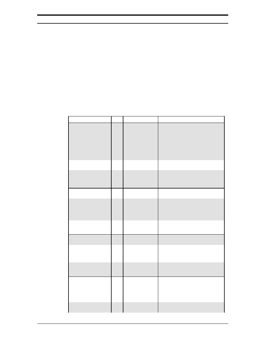
Table 3-4
Signal Description
Signal Name
Dir.
Pin
Description
A10 – A00
(PC Card Memory Mode)
I
8,10,11,12,
14,15,16,17,
18,19,20
These address lines along with the -REG
signal are used to select the following:
The I/O port address registers within the
CompactFlash Storage Card or CF+ Card,
the memory mapped port address
registers within the CompactFlash Storage
Card or CF+ Card, a byte in the card's
information structure and its configuration
control and status registers.
A10 – A00
(PC Card I/O Mode)
This signal is the same as the PC Card
Memory Mode signal.
A02 - A00
(True IDE Mode)
I
18,19,20
In True IDE Mode, only A [02:00] are used
to select the one of eight registers in the
Task File, the remaining address lines
should be grounded by the host.
BVD1
(PC Card Memory Mode)
I/O
46
This signal is asserted high, as BVD1 is
not supported.
-STSCHG
(PC Card I/O Mode)
Status Changed
This signal is asserted low to alert the host
to changes in the READY and Write
Protect states, while the I/O interface is
configured. Its use is controlled by the
Card Config and Status Register.
-PDIAG
(True IDE Mode)
In the True IDE Mode, this input / output is
the Pass Diagnostic signal in the Master /
Slave handshake protocol.
BVD2
(PC Card Memory Mode)
I/O
45
This signal is asserted high, as BVD2 is
not supported.
-SPKR
(PC Card I/O Mode)
This line is the Binary Audio output from
the card. If the Card does not support the
Binary Audio function, this line should be
held negated.
-DASP
(True IDE Mode)
In the True IDE Mode, this input/output is
the Disk Active/Slave Present signal in the
Master/Slave handshake protocol.
-CD1, -CD2
(PC Card Memory Mode)
O
26,25
These Card Detect pins are connected to
ground on the CompactFlash Storage
Card or CF+ Card. They are used by the
host to determine that the CompactFlash
Storage Card or CF+ Card is fully inserted
into its socket.
-CD1, -CD2
(PC Card I/O Mode)
This signal is the same for all modes.
相关PDF资料 |
PDF描述 |
|---|---|
| SDCFAB-008G | IDE COMPATIBLE, FLASH MEMORY DRIVE CONTROLLER, XMA50 |
| SDCFAA-002G | IDE COMPATIBLE, FLASH MEMORY DRIVE CONTROLLER, XMA50 |
| SDCFB-16-101 | FLASH MEMORY DRIVE CONTROLLER, XMA50 |
| SDCF2B-300-101 | FLASH MEMORY DRIVE CONTROLLER, XMA |
| SDCFBI-48-101 | FLASH MEMORY DRIVE CONTROLLER, XMA50 |
相关代理商/技术参数 |
参数描述 |
|---|---|
| SDCFB16101 | 制造商:SAND 功能描述: |
| SDCFB1610100 | 制造商:SanDisk Corporation 功能描述: |
| SDCFB-16-101-50 | 制造商:SanDisk Corporation 功能描述:Compactflash |
| SDCFB-2048-201-01 | 制造商:SanDisk Corporation 功能描述:2048MB Standard Grade CompactFlash |
| SDCFB-256-201-80 | 制造商:SanDisk Corporation 功能描述:256MB 50P CF COMPACTFLASH CARD INDUSTRIAL GRADE CLAM |
发布紧急采购,3分钟左右您将得到回复。