- 您现在的位置:买卖IC网 > PDF目录69341 > SED1241DAB 24 X 80 DOTS DOT MAT LCD DRVR AND DSPL CTLR, UUC210 PDF资料下载
参数资料
| 型号: | SED1241DAB |
| 元件分类: | 显示控制器 |
| 英文描述: | 24 X 80 DOTS DOT MAT LCD DRVR AND DSPL CTLR, UUC210 |
| 封装: | DIE-210 |
| 文件页数: | 6/67页 |
| 文件大小: | 736K |
| 代理商: | SED1241DAB |
第1页第2页第3页第4页第5页当前第6页第7页第8页第9页第10页第11页第12页第13页第14页第15页第16页第17页第18页第19页第20页第21页第22页第23页第24页第25页第26页第27页第28页第29页第30页第31页第32页第33页第34页第35页第36页第37页第38页第39页第40页第41页第42页第43页第44页第45页第46页第47页第48页第49页第50页第51页第52页第53页第54页第55页第56页第57页第58页第59页第60页第61页第62页第63页第64页第65页第66页第67页
8–14
EPSON
SED1240 Series
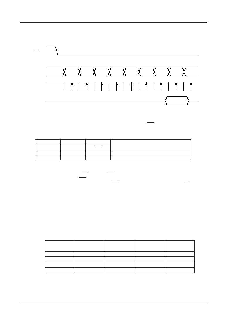
Fig. 1 shows a timing chart of the serial interface. In case of the SCL signal, extreme care should be taken about terminal
reflection and external noise due to a wiring length. Accordingly, it is recommended to make an operation check.
It is also recommended to periodically refresh the each command write state to prevent a malfunction from being caused
by noise.
Fig. 1 Serial Interface Input Timing
Identification of data bus signals
The SED1240 series identifies each data bus signal by a combination of A0 and WR (E) as shown in Table 3.
Table 3
Chip select
The SED1240 series has chip select pin CS. Only when CS = “L”, the MPU interface is enabled. In the other states than
the chip select state, D0 to D7 and A0, WR, SI, and SCL inputs are invalidated. When an serial input interface is selected,
the shift register and the counter are reset. However, the RES input can be performed regardless of the CS state.
Power Circuit
The power circuit built in the SED1240 series is a low power consumption power circuit that generates a voltage required
for liquid crystal drive, and consists of a boosting circuit, voltage regulating circuit, and voltage follower.
The power circuit capacity is set for a small-scale liquid crystal panel.
In the case of a liquid crystal panel with a large display capacity, the display quality may be remarkably degraded. In this
case, an external power supply is required.
Functional selection is performed by power control commands.
Some parts of the external power supply and the internal power supply can be used together.
Table 4
Note 1: When the boosting circuit is turned off, set the boosting system pins (CAP1+, CAP1–, CAP2+, CAP2–) to
OPEN so that liquid crystal drive voltages may be applied to the VOUT pin from the outside.
Note 2: When the voltage regulating circuit is not used with the boosting circuit OFF, set the VOUT pin and the
boosting system pins to OPEN and connect the V5 pin to give liquid crystal drive voltages from the outside.
Note 3: When all the built-in power supplies are turned off, liquid crystal drive voltages V1, V2, V3, V4, and V5 are
supplied from the outside and set the CAP1+, CAP1–, VSS2 and VOUT pins to OPEN.
D6 (SCL)
1
A0
D7 (SI)
CS
D7
D6
D5
D4
D3
D2
D1
D0
D7
23
456
7
81
Common
68 series
80 series
Function
A0
(E)
WR
1
0
Writes into the RAM and symbol register.
0
1
0
Writes into the internal register (commands)
Boosting
Voltage regulat-
Voltage
External
Boosting
circuit
ing circuit
follower
voltage input
system pin
q
VSS2
USE
×
q
VOUT, VSS2
OPEN
××
q
V5, VSS2
OPEN
×××
V1, V2, V3, V4, V5
OPEN
Note 1
Note 2
Note 3
相关PDF资料 |
PDF描述 |
|---|---|
| SED1241TXX | 24 X 80 DOTS DOT MAT LCD DRVR AND DSPL CTLR, UUC |
| SED1278D0G | 16 X 40 DOTS DOT MAT LCD DRVR AND DSPL CTLR, UUC |
| SED1278F0H | 16 X 40 DOTS DOT MAT LCD DRVR AND DSPL CTLR, PQFP80 |
| SED1278D | 16 X 40 DOTS DOT MAT LCD DRVR AND DSPL CTLR, UUC80 |
| SED1278F | 16 X 40 DOTS DOT MAT LCD DRVR AND DSPL CTLR, PQFP80 |
相关代理商/技术参数 |
参数描述 |
|---|---|
| SED1278 | 制造商:未知厂家 制造商全称:未知厂家 功能描述:CMOS DOT MATRIX LCD CONTROLLER DRIVER |
| SED1278D | 制造商:EPSON 制造商全称:EPSON 功能描述:Dot Matrix LCD Controller Driver |
| SED1278D0A | 制造商:未知厂家 制造商全称:未知厂家 功能描述:CMOS DOT MATRIX LCD CONTROLLER DRIVER |
| SED1278D0B | 制造商:未知厂家 制造商全称:未知厂家 功能描述:CMOS DOT MATRIX LCD CONTROLLER DRIVER |
| SED1278D0C | 制造商:未知厂家 制造商全称:未知厂家 功能描述:CMOS DOT MATRIX LCD CONTROLLER DRIVER |
发布紧急采购,3分钟左右您将得到回复。