- 您现在的位置:买卖IC网 > PDF目录69341 > SED1242DGB 16 X 80 DOTS DOT MAT LCD DRVR AND DSPL CTLR, UUC210 PDF资料下载
参数资料
| 型号: | SED1242DGB |
| 元件分类: | 显示控制器 |
| 英文描述: | 16 X 80 DOTS DOT MAT LCD DRVR AND DSPL CTLR, UUC210 |
| 封装: | DIE-210 |
| 文件页数: | 8/67页 |
| 文件大小: | 736K |
| 代理商: | SED1242DGB |
第1页第2页第3页第4页第5页第6页第7页当前第8页第9页第10页第11页第12页第13页第14页第15页第16页第17页第18页第19页第20页第21页第22页第23页第24页第25页第26页第27页第28页第29页第30页第31页第32页第33页第34页第35页第36页第37页第38页第39页第40页第41页第42页第43页第44页第45页第46页第47页第48页第49页第50页第51页第52页第53页第54页第55页第56页第57页第58页第59页第60页第61页第62页第63页第64页第65页第66页第67页
8–16
EPSON
SED1240 Series
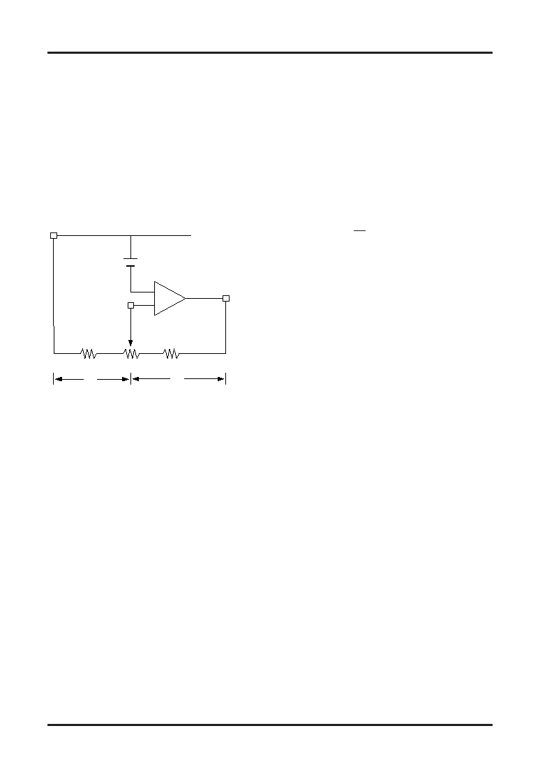
Voltage regulating circuit
The boosting voltage generated at VOUT is output as a
liquid crystal drive voltage of V5 through the voltage
regulating circuit.
The SED1240 series is provided with a high-precision
constant-voltage source, a 32-step electronic volume
function, and a V5 voltage regulating resistor. This
permits constructing a high-precision voltage regulating
circuit with a small quantity of parts. The voltage
regulating circuit outputs VEV and has a temperature
gradient of about –0.04%.
As the V5 voltage regulating resistor, a built-in resistor or
an external resistor can be selected by command as a
matter of configuration.
[When using an external resistor (No use of V5 voltage regulating built-in resistor is set by command.)]
The V5 voltage can be obtained from the following expression 1 by adjusting resistors Ra and Rb within the range of
| V5 | < | VOUT |.
R1
R2
R3
VR
V0
VDD
+
V5
VEV (constant-voltage source
+ electronic volume)
-
Ra
Rb
V5 = (1 +
Rb
) VEV
.............................. 1
Ra
In this case, VEV is determined by the constant-voltage
source in the IC and by setting the electronic volume.
When the electronic volume value is (00000), VREG =
2.0 V, being constant.
For voltage adjustment of V5 output, connect a variable
resistor among VR, VDD, and V5. For fine voltage
adjustment of V5 output, it is recommended to combine
fixed resistors R1 and R3 with variable resistor R2.
[R1, R2 and R3 setup example]
R1 + R2 + R3 = 1.2 M
(Determined by the current
value I05 flowing between VDD and V5. Supposing I05
≤ 5 A)
Minimum voltage of V5: –6 V (Determined by liquid
crystal characteristic)
Variable voltage range by R2: –4 to –6 V (Determined
by the liquid crystal characteristic)
When the electronic volume register is set to (0, 0, 0,
0, 0), VEV = 2.0 V (TYP). Accordingly, each resistor
value can be calculated by the above conditions and
expression 1 as follows.
R1 = 400 K
R2 = 200 K
R3 = 600 K
Note 1: The input impedance of the VR pin is high, so
it is necessary to take a proper measure against
noise for short wiring and shielding wiring.
相关PDF资料 |
PDF描述 |
|---|---|
| SED1240TXX | 32 X 80 DOTS DOT MAT LCD DRVR AND DSPL CTLR, UUC |
| SED1241DAB | 24 X 80 DOTS DOT MAT LCD DRVR AND DSPL CTLR, UUC210 |
| SED1241TXX | 24 X 80 DOTS DOT MAT LCD DRVR AND DSPL CTLR, UUC |
| SED1278D0G | 16 X 40 DOTS DOT MAT LCD DRVR AND DSPL CTLR, UUC |
| SED1278F0H | 16 X 40 DOTS DOT MAT LCD DRVR AND DSPL CTLR, PQFP80 |
相关代理商/技术参数 |
参数描述 |
|---|---|
| SED1278 | 制造商:未知厂家 制造商全称:未知厂家 功能描述:CMOS DOT MATRIX LCD CONTROLLER DRIVER |
| SED1278D | 制造商:EPSON 制造商全称:EPSON 功能描述:Dot Matrix LCD Controller Driver |
| SED1278D0A | 制造商:未知厂家 制造商全称:未知厂家 功能描述:CMOS DOT MATRIX LCD CONTROLLER DRIVER |
| SED1278D0B | 制造商:未知厂家 制造商全称:未知厂家 功能描述:CMOS DOT MATRIX LCD CONTROLLER DRIVER |
| SED1278D0C | 制造商:未知厂家 制造商全称:未知厂家 功能描述:CMOS DOT MATRIX LCD CONTROLLER DRIVER |
发布紧急采购,3分钟左右您将得到回复。