- 您现在的位置:买卖IC网 > PDF目录18227 > SI1902DL-T1-E3 (Vishay Siliconix)MOSFET N-CH DUAL 20V SC70-6 PDF资料下载
参数资料
| 型号: | SI1902DL-T1-E3 |
| 厂商: | Vishay Siliconix |
| 文件页数: | 2/9页 |
| 文件大小: | 0K |
| 描述: | MOSFET N-CH DUAL 20V SC70-6 |
| 产品目录绘图: | DL-T1-E3 Series SOT-363 |
| 标准包装: | 1 |
| 系列: | TrenchFET® |
| FET 型: | 2 个 N 沟道(双) |
| FET 特点: | 逻辑电平门 |
| 漏极至源极电压(Vdss): | 20V |
| 电流 - 连续漏极(Id) @ 25° C: | 660mA |
| 开态Rds(最大)@ Id, Vgs @ 25° C: | 385 毫欧 @ 660ma,4.5V |
| Id 时的 Vgs(th)(最大): | 1.5V @ 250µA |
| 闸电荷(Qg) @ Vgs: | 1.2nC @ 4.5V |
| 功率 - 最大: | 270mW |
| 安装类型: | 表面贴装 |
| 封装/外壳: | 6-TSSOP,SC-88,SOT-363 |
| 供应商设备封装: | SC-70-6 |
| 包装: | 标准包装 |
| 产品目录页面: | 1663 (CN2011-ZH PDF) |
| 其它名称: | SI1902DL-T1-E3DKR |
�� �
�
�Si1902DL�
�Vishay� Siliconix�
�SPECIFICATIONS� (T� J� =� 25� °C,� unless� otherwise� noted)�
�Parameter�
�Symbol�
�Test� Conditions�
�Min.�
�Typ.�
�Max.�
�Unit�
�Static�
�Gate� Threshold� Voltage�
�V� GS(th)�
�V� DS� =� V� GS� ,� I� D� =� 250� μA�
�0.6�
�1.5�
�V�
�Gate-Body� Leakage�
�Zero� Gate� Voltage� Drain� Current�
�On-State� Drain� Current� a�
�I� GSS�
�I� DSS�
�I� D(on)�
�V� DS� =� 0� V,� V� GS� =� ±� 12� V�
�V� DS� =� 16� V,� V� GS� =� 0� V�
�V� DS� =� 16� V� GS� =� 0� V,� T� J� =� 85°C�
�V� DS� ?� 5� V,� V� GS� =� 4.5� V�
�1�
�±� 100�
�1�
�5�
�nA�
�μA�
�A�
�Drain-Source� On-State� Resistance� a�
�Forward� Transconductance� a�
�R� DS(on)�
�g� fs�
�V� GS� =� 4.5� V,� I� D� =� 0.66� A�
�V� GS� =� 2.5� V,� I� D� =� 0.40� A�
�V� DS� =� 10� V,� I� D� =� 0.66� A�
�0.320�
�0.560�
�1.5�
�0.385�
�0.630�
�?�
�S�
�Diode� Forward� Voltage�
�a�
�V� SD�
�I� S� =� 0.23� A,� V� GS� =� 0� V�
�0.8�
�1.2�
�V�
�Dynamic�
�b�
�Total� Gate� Charge�
�Q� g�
�0.8�
�1.2�
�Gate-Source� Charge�
�Gate-Drain� Charge�
�Q� gs�
�Q� gd�
�V� DS� =� 10� V,� V� GS� =� 4.5� V,� I� D� =� 0.66� A�
�0.06�
�0.30�
�nC�
�Gate� Resistance�
�R� g�
�f� =� 1� MHz�
�0.2�
�1�
�1.7�
�?�
�Turn-On� Delay� Time�
�t� d(on)�
�10�
�20�
�Rise� Time�
�t� r�
�V� DD� =� 10� V,� R� L� =� 20� ?�
�16�
�30�
�Turn-Off� DelayTime�
�Fall� Time�
�Source-Drain� Reverse� Recovery� Time�
�t� d(off)�
�t� f�
�t� rr�
�I� D� ?� 0.5� A,� V� GEN� =� 4.5� V,� R� g� =� 6� ?�
�I� F� =� 0.23� A,� dI/dt� =� 100� A/μs�
�10�
�10�
�20�
�20�
�20�
�40�
�ns�
�Notes:�
�a.� Pulse� test;� pulse� width� ?� 300� μs,� duty� cycle� ?� 2� %.�
�b.� Guaranteed� by� design,� not� subject� to� production� testing.�
�Stresses� beyond� those� listed� under� “Absolute� Maximum� Ratings”� may� cause� permanent� damage� to� the� device.� These� are� stress� ratings� only,� and� functional� operation�
�of� the� device� at� these� or� any� other� conditions� beyond� those� indicated� in� the� operational� sections� of� the� specifications� is� not� implied.� Exposure� to� absolute� maximum�
�rating� conditions� for� extended� periods� may� affect� device� reliability.�
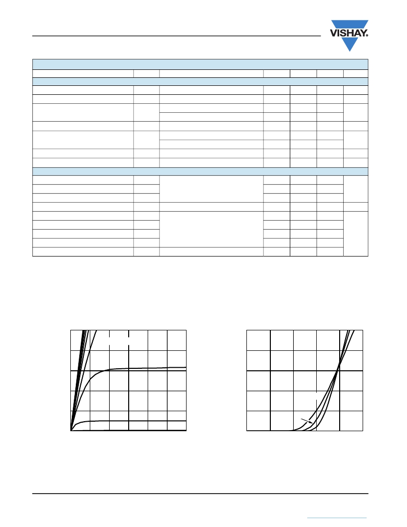
�TYPICAL� CHARACTERISTICS� (25� °C,� unless� otherwise� noted)�
�1.0�
�0.8�
�0.6�
�0.4�
�V� GS� =� 5� V� thru� 2.5� V�
�2V�
�1.0�
�0.8�
�0.6�
�0.4�
�T� C� =� 125� °C�
�0.2�
�0.0�
�1.5� V�
�1V�
�0.2�
�0.0�
�25 °C�
�-� 55� °C�
�0.0�
�0.5�
�1.0�
�1.5�
�2.0�
�2.5�
�3.0�
�0.0�
�0.5�
�1.0�
�1.5�
�2.0�
�2.5�
�www.vishay.com�
�2�
�V� DS� -� Drain-to-Source� Voltage� (V)�
�Output� Characteristics�
�V� GS� -� Gate-to-Source� Voltage� (V)�
�Transfer� Characteristics�
�Document� Number:� 71080�
�S11-2043-Rev.� J,� 17-Oct-11�
�This� document� is� subject� to� change� without� notice.�
�THE� PRODUCTS� DESCRIBED� HEREIN� AND� THIS� DOCUMENT� ARE� SUBJECT� TO� SPECIFIC� DISCLAIMERS,� SET� FORTH� AT� www.vishay.com/doc?91000�
�相关PDF资料 |
PDF描述 |
|---|---|
| M2047TYW03 | SWITCH ROCKER DP3T 6A 125V |
| FXO-LC738-150 | OSC 150 MHZ 3.3V LVDS SMD |
| FXO-LC738-155.52 | OSC 155.52 MHZ 3.3V LVDS SMD |
| B32676G3156K | CAP FILM 15UF 300VDC RADIAL |
| FXO-LC738-156.25 | OSC 156.25 MHZ 3.3V LVDS SMD |
相关代理商/技术参数 |
参数描述 |
|---|---|
| SI1902DL-T1-E3 | 制造商:Vishay Siliconix 功能描述:MOSFET |
| SI1902DL-T1-GE3 | 功能描述:MOSFET N-CH G-S 20V DUAL SC-70-6 RoHS:是 类别:分离式半导体产品 >> FET - 阵列 系列:TrenchFET® 产品目录绘图:8-SOIC Mosfet Package 标准包装:1 系列:- FET 型:2 个 N 沟道(双) FET 特点:逻辑电平门 漏极至源极电压(Vdss):60V 电流 - 连续漏极(Id) @ 25° C:3A 开态Rds(最大)@ Id, Vgs @ 25° C:75 毫欧 @ 4.6A,10V Id 时的 Vgs(th)(最大):3V @ 250µA 闸电荷(Qg) @ Vgs:20nC @ 10V 输入电容 (Ciss) @ Vds:- 功率 - 最大:1.4W 安装类型:表面贴装 封装/外壳:PowerPAK? SO-8 供应商设备封装:PowerPAK? SO-8 包装:Digi-Reel® 产品目录页面:1664 (CN2011-ZH PDF) 其它名称:SI7948DP-T1-GE3DKR |
| SI1902DL-T3 | 制造商:Vishay Intertechnologies 功能描述:Trans MOSFET N-CH 20V 0.66A 6-Pin SC-70 T/R |
| SI1903DL | 制造商:VISHAY 制造商全称:Vishay Siliconix 功能描述:Dual P-Channel 2.5-V (G-S) MOSFET |
| SI1903DL_08 | 制造商:VISHAY 制造商全称:Vishay Siliconix 功能描述:Dual P-Channel 2.5-V (G-S) MOSFET |
发布紧急采购,3分钟左右您将得到回复。