- 您现在的位置:买卖IC网 > Datasheet目录356 > SI3402-EVB (Silicon Laboratories Inc)BOARD EVAL POE FOR SI3402 Datasheet资料下载
参数资料
| 型号: | SI3402-EVB |
| 厂商: | Silicon Laboratories Inc |
| 文件页数: | 7/22页 |
| 文件大小: | 0K |
| 描述: | BOARD EVAL POE FOR SI3402 |
| 标准包装: | 1 |
| 主要目的: | 特殊用途 DC/DC,以太网供电(POE) |
| 输出及类型: | 1,非隔离 |
| 输出电压: | 5V |
| 输入电压: | 44 ~ 57 V |
| 稳压器拓扑结构: | 降压 |
| 频率 - 开关: | 350kHz |
| 板类型: | 完全填充 |
| 已供物品: | 板,CD |
| 已用 IC / 零件: | Si3402 |
| 其它名称: | 336-1827 |
�� �
�
�Si3402�
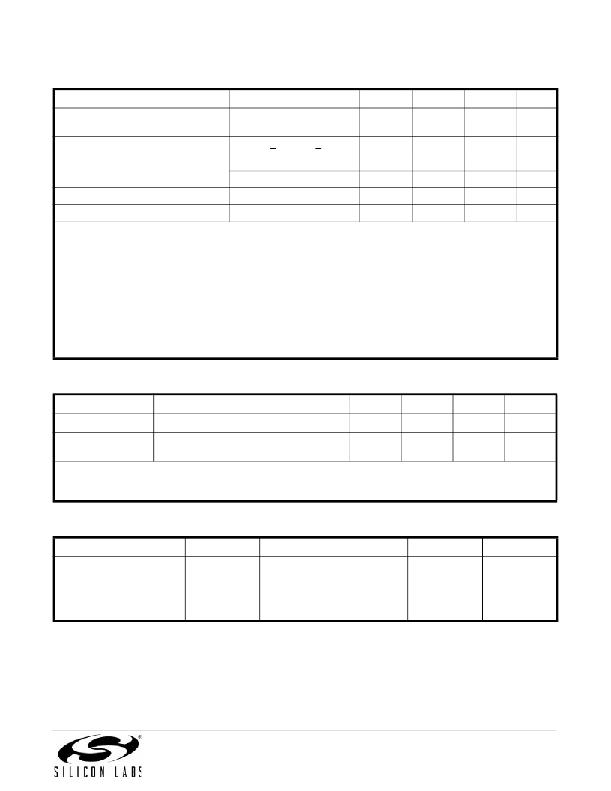
�Table� 4.� Electrical� Characteristics� (Continued)�
�Parameter�
�Description�
�Min�
�Typ�
�Max�
�Unit�
�Regulated� Output� Voltage� Tolerance�
�VDD� Accuracy� @� 0.8� mA�
�Softstart� Charging� Current�
�Thermal� Shutdown�
�Thermal� Shutdown� Hysteresis�
�6�
�Output� voltage� tolerance� @�
�VOUT�
�36� V� <� VPORT� <� 57� V�
�SSFT� pin�
�ISOSSFT� pin�
�Junction� temperature�
�–5�
�4.5�
�—�
�—�
�—�
�—�
�—�
�—�
�25�
�13�
�160�
�—�
�5�
�5.5�
�—�
�—�
�—�
�25�
�%�
�V�
�μA�
�μA�
�oC�
�oC�
�Notes:�
�1.� Transient� surge� defined� in� IEC60060� as� a� 1000� V� impulse� of� either� polarity� applied� to� CT1–CT2� or� SP1–SP2.� The�
�shape� of� the� impulse� shall� have� a� 300� ns� full� rise� time� and� a� 50� μs� half� fall� time� with� 201� ?� source� impedance.�
�2.� The� classification� currents� are� guaranteed� only� when� recommended� RCLASS� resistors� are� used,� as� specified� in�
�Table� 10.�
�3.� IPORT� includes� full� operating� current� of� switching� regulator� controller.�
�4.� The� PD� interface� includes� dual-level� input� current� limit.� At� turn-on,� before� the� HSO� load� capacitor� is� charged,� the�
�current� limit� is� set� at� the� inrush� level.� After� the� capacitor� has� been� charged� within� ~1.25� V� of� VNEG,� the� operating�
�current� limit� is� engaged.� This� higher� current� limit� remains� active� until� the� UVLO� lower� limit� has� been� tripped� or� until� the�
�hotswap� switch� is� sufficiently� current-limited� to� cause� a� foldback� of� the� HSO� voltage.�
�5.� See� “AN296:� Using� the� Si3400/1/2� PoE� PD� Controller� in� Isolated� and� Non-Isolated� Designs”� for� more� information.�
�6.� Applies� to� non-isolated� applications� only� (VOUT� on� schematic� in� Figure� 1).�
�Table� 5.� Total� Power� Dissipation�
�Description�
�Power� Dissipation�
�Power� Dissipation*�
�Test� Condition�
�VPORT� =� 50� V,� V� OUT� =� 5� V,� 2� A�
�VPORT� =� 50� V,� V� OUT� =� 5� V,� 2� A� w/� diode�
�bridges� bypassed�
�Min�
�—�
�—�
�Typ�
�1.2�
�0.7�
�Max�
�—�
�—�
�Unit�
�W�
�W�
�*Note:� Silicon� Laboratories� recommends� the� on-chip� diode� bridges� be� bypassed� when� output� power� requirements� are� >7� W�
�or� in� thermally-constrained� applications.� For� more� information,� see� “AN313:� Using� the� Si3402� in� High� Power�
�Applications”.�
�Table� 6.� Package� Thermal� Characteristics�
�Parameter�
�Symbol�
�Test� Condition�
�Typ�
�Unit�
�Still� air;� assumes� a� minimum� of�
�Thermal� Resistance�
�(Junction� to� Ambient)�
�?� JA�
�nine� thermal� vias� are� connected�
�to� a� 2� in� 2� heat� spreader� plane�
�for� the� package� “pad”� node�
�44�
�°C/W�
�(VNEG).�
�Rev.� 1.31�
�7�
�相关PDF资料 |
PDF描述 |
|---|---|
| SI3460-EVB | BOARD EVAL POE FOR SI3460 |
| SI8220BD-A-IS | IC ISODRIVER 2.5A OPTO IN 16SOIC |
| SI8402AB-B-IS | IC I2C ISOLATOR BIDIR 8-SOIC |
| SI8405AB-A-IS1 | IC ISOLATOR 10M 6CH 2.5K 16SOIC |
| SI8423BD-B-IS | ISOLATOR 2CH 5KV 150M 16SOIC |
相关代理商/技术参数 |
参数描述 |
|---|---|
| Si3402ISO-EVB | 功能描述:电源管理IC开发工具 PoE Pwrd-Isolated Low-EMI Eval Board RoHS:否 制造商:Maxim Integrated 产品:Evaluation Kits 类型:Battery Management 工具用于评估:MAX17710GB 输入电压: 输出电压:1.8 V |
| SI3403-A-GM | 制造商:Silicon Laboratories Inc 功能描述:POE POWERED DEVICE (UP TO 17W, LOW-EMI) - RECOMMENDED FOR AL - Trays 制造商:Silicon Laboratories Inc 功能描述:IC POE CTLR TO 17W LOW EMI 20QFN 制造商:Silicon Laboratories Inc 功能描述:PoE Powered Device (up to 17W, low-EMI) |
| Si3403-A-GMR | 制造商:Silicon Laboratories Inc 功能描述:POE POWERED DEVICE (UP TO 17W, LOW-EMI) - RECOMMENDED FOR AL - Tape and Reel 制造商:Silicon Laboratories Inc 功能描述:PoE Powered Device (up to 17W, low-EMI) |
| SI3403DV-T1-E3 | 功能描述:MOSFET 20V 5.0A 3.2W RoHS:否 制造商:STMicroelectronics 晶体管极性:N-Channel 汲极/源极击穿电压:650 V 闸/源击穿电压:25 V 漏极连续电流:130 A 电阻汲极/源极 RDS(导通):0.014 Ohms 配置:Single 最大工作温度: 安装风格:Through Hole 封装 / 箱体:Max247 封装:Tube |
| SI3403DV-T1-GE3 | 功能描述:MOSFET 20V 5.0A 3.2W 70mohm @ 4.5V RoHS:否 制造商:STMicroelectronics 晶体管极性:N-Channel 汲极/源极击穿电压:650 V 闸/源击穿电压:25 V 漏极连续电流:130 A 电阻汲极/源极 RDS(导通):0.014 Ohms 配置:Single 最大工作温度: 安装风格:Through Hole 封装 / 箱体:Max247 封装:Tube |
发布紧急采购,3分钟左右您将得到回复。