- 您现在的位置:买卖IC网 > PDF目录2016 > SI5020-B-GM (Silicon Laboratories Inc)IC CLK DATA REC SONET/SDH 20-QFN PDF资料下载
参数资料
| 型号: | SI5020-B-GM |
| 厂商: | Silicon Laboratories Inc |
| 文件页数: | 3/22页 |
| 文件大小: | 0K |
| 描述: | IC CLK DATA REC SONET/SDH 20-QFN |
| 标准包装: | 75 |
| 系列: | SiPHY™, DSPLL® |
| 类型: | 时钟和数据恢复(CDR) |
| PLL: | 是 |
| 主要目的: | 以太网,SONET/SDH,ATM 应用 |
| 输入: | 时钟 |
| 输出: | CML |
| 电路数: | 1 |
| 比率 - 输入:输出: | 1:2 |
| 差分 - 输入:输出: | 是/是 |
| 频率 - 最大: | 2.7GHz |
| 电源电压: | 2.375 V ~ 2.625 V |
| 工作温度: | -40°C ~ 85°C |
| 安装类型: | 表面贴装 |
| 封装/外壳: | 20-VFQFN 裸露焊盘 |
| 供应商设备封装: | 20-QFN(4x4) |
| 包装: | 管件 |
Si5020
Rev. 1.5
11
4. Functional Description
The Si5020 utilizes a phase-locked loop (PLL) to
recover a clock synchronous to the input data stream.
This clock is used to retime the data, and both the
recovered clock and data are output synchronously via
current
mode
logic
(CML)
drivers.
Optimal
jitter
performance is obtained by using Silicon Laboratories'
DSPLL technology to eliminate the noise entry points
caused by external PLL loop filter components.
4.1. DSPLL
The PLL structure (shown in Figure 1 on page 5) utilizes
Silicon Laboratories' DSPLL technology to eliminate the
need for external loop filter components found in
traditional PLL implementations. This is achieved by
using a digital signal processing (DSP) algorithm to
replace the loop filter commonly found in analog PLL
designs. This algorithm processes the phase detector
error term and generates a digital control value to adjust
the frequency of the voltage-controlled oscillator (VCO).
Because external loop filter components are not
required, sensitive noise entry points are eliminated,
making the DSPLL less susceptible to board-level noise
sources that make SONET/SDH jitter compliance
difficult to attain.
4.2. PLL Self-Calibration
The Si5020 achieves optimal jitter performance by
using self-calibration circuitry to set the loop gain
parameters within the DSPLL. For the self-calibration
circuitry to operate correctly, the power supply voltage
must exceed 2.25 V when calibration occurs. For best
performance, the user should force a self-calibration
once the supply has stabilized on powerup.
A self-calibration can be initiated by forcing a high-to-
low transition on the powerdown control input, PWRDN/
CAL, while a valid reference clock is supplied to the
REFCLK input. The PWRDN/CAL input should be held
high at least 1
s before transitioning low to guarantee a
self-calibration. Several application circuits that could be
used to initiate a power-on self-calibration are provided
in Silicon Laboratories’ “AN42: Controlling DSPLL
Self-Calibration for the Si5020/5018/5010 CDR Devices
and Si531x Clock Multiplier/Regenerator Devices.”
4.3. Multi-Rate Operation
The Si5020 supports clock and data recovery for OC-48
and STM-16 data streams. In addition, the PLL was
designed to operate at data rates up to 2.7 Gbps to
support
OC-48/STM-16
applications
that
employ
forward error correction (FEC).
Multi-rate operation is achieved by configuring the
device to divide down the output of the VCO to the
desired data rate. The divide factor is configured by the
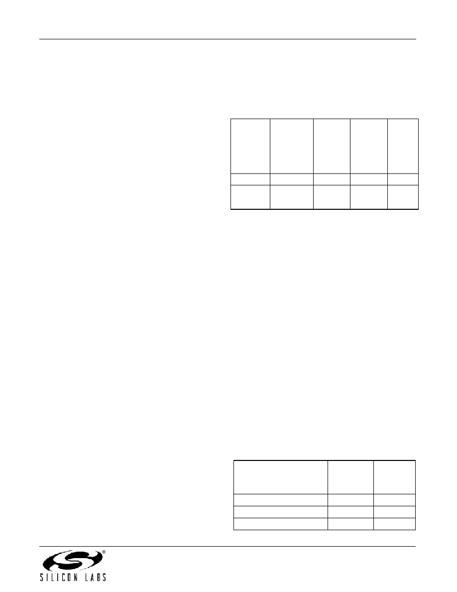
RATESEL0-1 pins. The RATESEL0-1 configuration and
associated data rates are given in Table 7.
4.4. Reference Clock Detect
The Si5020 CDR requires an external reference clock
applied to the REFCLK input for normal device
operation. When REFCLK is absent, the LOL alarm will
always be asserted when it has been determined that
no activity exists on REFCLK, indicating the frequency
lock status of the PLL is unknown. Additionally, the
Si5020 uses the reference clock to center the VCO
output frequency so that clock and data can be
recovered from the input data stream. The device self
configures for operation with one of three reference
clock frequencies. This eliminates the need to externally
configure the device to operate with a particular
reference clock.
The reference clock centers the VCO for a nominal
output of between 2.5 GHz and 2.7 GHz. The VCO
frequency is centered at 16, 32, or 128 times the
reference
clock
frequency.
Detection
circuitry
continuously monitors the reference clock input to
determine whether the device should be configured for
a reference clock that is 1/16, 1/32, or 1/128 the
nominal VCO output. Approximate reference clock
frequencies for some target applications are given in
Table 8.
Table 7. Multi-Rate Configuration
RATESEL
[0:1]
SONET/
SDH
Gigabit
Ethernet
OC-48
with
15/14
FEC
CLK
Divider
00
2.488 Gbps
—
2.67 Gbps
1
10
1.244 Gbps
1.25 Gbps
—
2
01
622.08 Mbps
—
4
11
155.52 Mbps
—
16
Table 8. Typical REFCLK Frequencies
SONET/SDH
Gigabit
Ethernet
SONET/
SDH with
15/14 FEC
Ratio of
VCO to
REFCLK
19.44 MHz
19.53 MHz
20.83 MHz
128
77.76 MHz
78.125 MHz
83.31 MHz
32
155.52 MHz
156.25 MHz
166.63 MHz
16
相关PDF资料 |
PDF描述 |
|---|---|
| SI5023-D-GM | IC CLOCK/DATA RECVRY W/AMP 28MLP |
| SI52142-A01AGM | IC CLK GENERATOR 200MHZ 24QFN |
| SI52143-A01AGM | IC CLK GEN QUAD PCIE 24QFN |
| SI52144-A01AGM | IC CLK GENERATOR 100MHZ 24QFN |
| SI5315A-C-GM | IC CLK MULT 8KHZ-644.53MHZ 36QFN |
相关代理商/技术参数 |
参数描述 |
|---|---|
| SI5020-B-GMR | 功能描述:计时器和支持产品 Multi-Rate SONET SDH CDR RoHS:否 制造商:Micrel 类型:Standard 封装 / 箱体:SOT-23 内部定时器数量:1 电源电压-最大:18 V 电源电压-最小:2.7 V 最大功率耗散: 最大工作温度:+ 85 C 最小工作温度:- 40 C 封装:Reel |
| SI5020-BM | 功能描述:计时器和支持产品 SNT/SDH GbE 2.7Gbps OC48/12/3 STM16/4/1 RoHS:否 制造商:Micrel 类型:Standard 封装 / 箱体:SOT-23 内部定时器数量:1 电源电压-最大:18 V 电源电压-最小:2.7 V 最大功率耗散: 最大工作温度:+ 85 C 最小工作温度:- 40 C 封装:Reel |
| SI5020-BMR | 功能描述:计时器和支持产品 SNT/SDH GbE 2.7Gbps OC48/12/3 STM16/4/1 RoHS:否 制造商:Micrel 类型:Standard 封装 / 箱体:SOT-23 内部定时器数量:1 电源电压-最大:18 V 电源电压-最小:2.7 V 最大功率耗散: 最大工作温度:+ 85 C 最小工作温度:- 40 C 封装:Reel |
| SI5020C-BA | 功能描述:时钟和定时器开发工具 Multi-Rate SONET/ SDH CDR Morph Board RoHS:否 制造商:Texas Instruments 产品:Evaluation Modules 类型:Clock Conditioners 工具用于评估:LMK04100B 频率:122.8 MHz 工作电源电压:3.3 V |
| SI5020C-BAR | 制造商:Silicon Laboratories Inc 功能描述: |
发布紧急采购,3分钟左右您将得到回复。