- 您现在的位置:买卖IC网 > PDF目录16484 > SI5316-EVB (Silicon Laboratories Inc)BOARD EVAL FOR SI5316 PDF资料下载
参数资料
| 型号: | SI5316-EVB |
| 厂商: | Silicon Laboratories Inc |
| 文件页数: | 1/26页 |
| 文件大小: | 0K |
| 描述: | BOARD EVAL FOR SI5316 |
| 标准包装: | 1 |
| 主要目的: | 计时,时钟发生器 |
| 已用 IC / 零件: | SI5316 |
| 已供物品: | 板,线缆,CD,文档 |
Rev. 1.0 7/12
Copyright 2012 by Silicon Laboratories
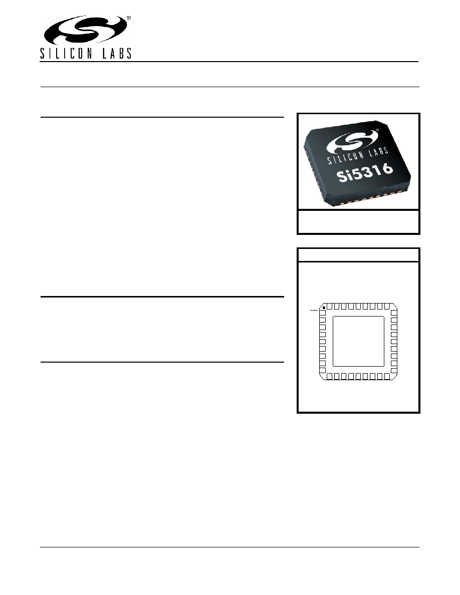
Si5316
P RECISION C LOCK J ITTER A TTENUATOR
Features
Applications
Description
The Si5316 is a low jitter, precision jitter attenuator for high-speed
communication systems, including OC-48, OC-192, 10G Ethernet, and
10G Fibre Channel. The Si5316 accepts dual clock inputs in the 19, 38,
77, 155, 311, or 622 MHz frequency range and generates a jitter-
attenuated clock output at the same frequency. Within each of these clock
ranges, the device can be tuned approximately 15% higher than nominal
SONET/SDH frequencies, up to a maximum of 710 MHz in the 622 MHz
range. The Si5316 is based on Silicon Laboratories' 3rd-generation
DSPLL technology, which provides any-frequency synthesis and jitter
attenuation in a highly integrated PLL solution that eliminates the need for
external VCXO and loop filter components. The DSPLL loop bandwidth is
digitally programmable, providing jitter performance optimization at the
application level. Operating from a single 1.8, 2.5, or 3.3 V supply, the
Si5316 is ideal for providing jitter attenuation in high performance timing
applications.
Fixed frequency jitter attenuator
with selectable clock ranges at
19, 38, 77, 155, 311, and
622 MHz (710 MHz max)
Support for SONET, 10GbE,
10GFC, and corresponding FEC
rates
Ultra-low jitter clock output with
jitter generation as low as
0.3 psRMS (50 kHz–80 MHz)
Integrated loop filter with
selectable loop bandwidth
(100 Hz–7.9 kHz)
Meets OC-192 GR-253-CORE
jitter specifications
Dual clock inputs with integrated
clock select mux
One clock input can be 1x, 4x, or
32x the frequency of the second
clock input
Single clock output with
selectable signal format:
LVPECL, LVDS, CML, CMOS
LOL, LOS alarm outputs
Pin programmable settings
On-chip voltage regulator for 1.8
±5%, 2.5 ±10%, or 3.3 V ±10%
operation
Small size (6 x 6 mm 36-lead
QFN)
Pb-free, RoHS compliant
Optical modules
SONET/SDH OC-48/OC-192/
STM-16/STM-64 line cards
10GbE, 10GFC line cards
ITU G.709 line cards
Wireless basestations
Test and measurement
Synchronous Ethernet
Patents pending
Ordering Information:
See page 20.
Pin Assignments
1
2
3
29
30
31
32
33
34
35
36
20
21
22
23
24
25
26
27
10 11 12 13 14 15 16 17
4
5
6
7
8
NC
RST
C2B
C1B
GND
VDD
XA
VD
D
RATE0
CK
IN
2
+
CKIN2–
DBL_B
Y
RATE1
CKIN1+
CKIN1–
CS
BWSEL0
BWSEL1
FRQSEL
CK1DIV
CK2DIV
NC
SFO
U
T1
GND
VDD
SF
OUT
0
CKOUT
–
CKOUT
+
NC
GND
Pad
FRQSEL0
GND
9
18
19
28
XB
LO
L
GND
NC
Si5316
相关PDF资料 |
PDF描述 |
|---|---|
| 1-6278027-4 | C/A ST/MT-RJ, MM 14 M1 |
| 2-5492191-5 | CA SM LDS SCAPC-SC/UPC(NG) |
| ECM25DRXH | CONN EDGECARD 50POS DIP .156 SLD |
| H1AXH-5036M | IDC CABLE - HSC50H/AE50M/X |
| RCM24DRPH | CONN EDGECARD 48POS DIP .156 SLD |
相关代理商/技术参数 |
参数描述 |
|---|---|
| SI5317 | 制造商:SILABS 制造商全称:SILABS 功能描述:Pin-Controlled 1_710 MHz Jitter Cleaning Clock |
| Si5317A-C-GM | 功能描述:标准时钟振荡器 Pin-Program. Jitter Cleaning Clock RoHS:否 制造商:AVX 产品:Standard Clock Oscillators 封装 / 箱体:7 mm x 5 mm 频率:75 MHz 频率稳定性:50 PPM 电源电压:2.5 V 负载电容: 端接类型:SMD/SMT 最小工作温度:0 C 最大工作温度:+ 70 C 输出格式:LVDS 尺寸: 封装:Reel 系列: |
| SI5317A-C-GMR | 功能描述:时钟合成器/抖动清除器 Pin-Program Jitter Clean Clk 1In/2Out RoHS:否 制造商:Skyworks Solutions, Inc. 输出端数量: 输出电平: 最大输出频率: 输入电平: 最大输入频率:6.1 GHz 电源电压-最大:3.3 V 电源电压-最小:2.7 V 封装 / 箱体:TSSOP-28 封装:Reel |
| Si5317B-C-GM | 功能描述:标准时钟振荡器 Pin-Program. Jitter Cleaning Clock RoHS:否 制造商:AVX 产品:Standard Clock Oscillators 封装 / 箱体:7 mm x 5 mm 频率:75 MHz 频率稳定性:50 PPM 电源电压:2.5 V 负载电容: 端接类型:SMD/SMT 最小工作温度:0 C 最大工作温度:+ 70 C 输出格式:LVDS 尺寸: 封装:Reel 系列: |
| SI5317B-C-GMR | 功能描述:时钟合成器/抖动清除器 Pin-Program Jitter Clean Clk 1In/2Out RoHS:否 制造商:Skyworks Solutions, Inc. 输出端数量: 输出电平: 最大输出频率: 输入电平: 最大输入频率:6.1 GHz 电源电压-最大:3.3 V 电源电压-最小:2.7 V 封装 / 箱体:TSSOP-28 封装:Reel |
发布紧急采购,3分钟左右您将得到回复。