- 您现在的位置:买卖IC网 > PDF目录8986 > SI5322-C-GM (Silicon Laboratories Inc)IC PREC CLOCK MULTIPLIER 36-QFN PDF资料下载
参数资料
| 型号: | SI5322-C-GM |
| 厂商: | Silicon Laboratories Inc |
| 文件页数: | 7/24页 |
| 文件大小: | 0K |
| 描述: | IC PREC CLOCK MULTIPLIER 36-QFN |
| 标准包装: | 490 |
| 系列: | DSPLL® |
| 类型: | 时钟乘法器 |
| PLL: | 是 |
| 输入: | 时钟 |
| 输出: | CML,CMOS,LVDS,LVPECL |
| 电路数: | 1 |
| 比率 - 输入:输出: | 2:2 |
| 差分 - 输入:输出: | 是/是 |
| 频率 - 最大: | 1.05GHz |
| 除法器/乘法器: | 无/是 |
| 电源电压: | 1.71 V ~ 3.63 V |
| 工作温度: | -40°C ~ 85°C |
| 安装类型: | 表面贴装 |
| 封装/外壳: | 36-VFQFN 裸露焊盘 |
| 供应商设备封装: | 36-QFN(6x6) |
| 包装: | 托盘 |
Si5322
Rev. 0.51
15
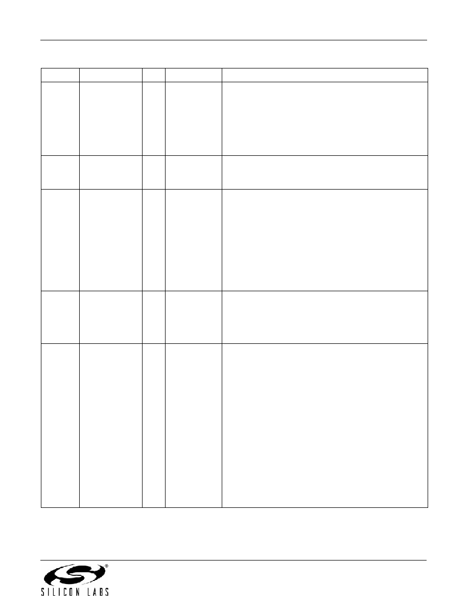
5, 10, 11,
15, 32
VDD
Supply
Supply.
The device operates from a 1.8, 2.5, or 3.3 V supply. Bypass
capacitors should be associated with the following VDD pins:
5
0.1 F
10
0.1 F
32
0.1 F
A 1.0 F should be placed as close to device as is practical.
6, 8,19,
20, 31
GND
Supply
Ground.
Must be connected to system ground. Minimize the ground
path impedance for optimal performance of this device.
9
AUTOSEL
I
3-Level
Manual/Automatic Clock Selection.
Three level input that selects the method of input clock
selection to be used.
L = Manual.
M = Automatic non-revertive.
H = Automatic revertive.
The pin has a weak pull-up and weak pull-down and
defaults to M.
Some designs may require an external resistor voltage
divider when driven by an active device that will tri-state.
12
13
CKIN2+
CKIN2–
IMulti
Clock Input 2.
Differential input clock. This input can also be driven with a
single-ended signal. Input frequency selected from a table
of values. The same frequency must be applied to CKIN1
and CKIN2.
14
DBL2_BY
I
3-Level
Output 2 Disable/Bypass Mode Control.
Controls enable of CKOUT2 divider/output buffer path and
PLL bypass mode.
L = CKOUT2 enabled.
M = CKOUT2 disabled.
H = Bypass mode with CKOUT2 enabled.
CMOS outputs do not support Bypass Mode.
The pin has a weak pull-up and weak pull-down and
defaults to M.
Some designs may require an external resistor voltage
divider when driven by an active device that will tri-state.
16
17
CKIN1+
CKIN1–
IMulti
Clock Input 1.
Differential input clock. This input can also be driven with a
single-ended signal. Input frequency selected from a table
of values. The same frequency must be applied to CKIN1
and CKIN2.
Table 9. Si5322 Pin Descriptions (Continued)
Pin #
Pin Name
I/O
Signal Level
Description
相关PDF资料 |
PDF描述 |
|---|---|
| LTC1453CS8#PBF | IC D/A CONV 12BIT R-R 8-SOIC |
| VI-B01-MY-F2 | CONVERTER MOD DC/DC 12V 50W |
| VI-B01-MY-F1 | CONVERTER MOD DC/DC 12V 50W |
| VI-B00-MY-F3 | CONVERTER MOD DC/DC 5V 50W |
| VI-B00-MY-F1 | CONVERTER MOD DC/DC 5V 50W |
相关代理商/技术参数 |
参数描述 |
|---|---|
| SI5322-C-GMR | 功能描述:时钟发生器及支持产品 Pin-Ctrl Precision Clk Xplier 2/2 RoHS:否 制造商:Silicon Labs 类型:Clock Generators 最大输入频率:14.318 MHz 最大输出频率:166 MHz 输出端数量:16 占空比 - 最大:55 % 工作电源电压:3.3 V 工作电源电流:1 mA 最大工作温度:+ 85 C 安装风格:SMD/SMT 封装 / 箱体:QFN-56 |
| SI5323 | 制造商:SILABS 制造商全称:SILABS 功能描述:Pin-Controlled 1_710 MHz Jitter Cleaning Clock |
| Si5323-B-GM | 功能描述:锁相环 - PLL PIN-PROGRAMMABLE CLK MULT / JITTER ATTEN RoHS:否 制造商:Silicon Labs 类型:PLL Clock Multiplier 电路数量:1 最大输入频率:710 MHz 最小输入频率:0.002 MHz 输出频率范围:0.002 MHz to 808 MHz 电源电压-最大:3.63 V 电源电压-最小:1.71 V 最大工作温度:+ 85 C 最小工作温度:- 40 C 封装 / 箱体:QFN-36 封装:Tray |
| SI5323-B-GMR | 制造商:Silicon Laboratories Inc 功能描述:PIN-PROGRAMMABLE PRECISION CLOCK MULTIPLIER/JITTER ATTENUATO - Tape and Reel |
| Si5323-C-GM | 功能描述:锁相环 - PLL PIN-PROGRAMMABLE CLK MULT / JITTER ATTEN RoHS:否 制造商:Silicon Labs 类型:PLL Clock Multiplier 电路数量:1 最大输入频率:710 MHz 最小输入频率:0.002 MHz 输出频率范围:0.002 MHz to 808 MHz 电源电压-最大:3.63 V 电源电压-最小:1.71 V 最大工作温度:+ 85 C 最小工作温度:- 40 C 封装 / 箱体:QFN-36 封装:Tray |
发布紧急采购,3分钟左右您将得到回复。