- 您现在的位置:买卖IC网 > PDF目录98080 > SI5334B-A00123-GM (SILICON LABORATORIES) PLL BASED CLOCK DRIVER, QCC24 PDF资料下载
参数资料
| 型号: | SI5334B-A00123-GM |
| 厂商: | SILICON LABORATORIES |
| 元件分类: | 时钟及定时 |
| 英文描述: | PLL BASED CLOCK DRIVER, QCC24 |
| 封装: | 4 X 4 MM, ROHS COMPLIANT, MO-220VGGD-8, QFN-24 |
| 文件页数: | 13/34页 |
| 文件大小: | 233K |
| 代理商: | SI5334B-A00123-GM |
第1页第2页第3页第4页第5页第6页第7页第8页第9页第10页第11页第12页当前第13页第14页第15页第16页第17页第18页第19页第20页第21页第22页第23页第24页第25页第26页第27页第28页第29页第30页第31页第32页第33页第34页
Si5334
20
Preliminary Rev. 0.16
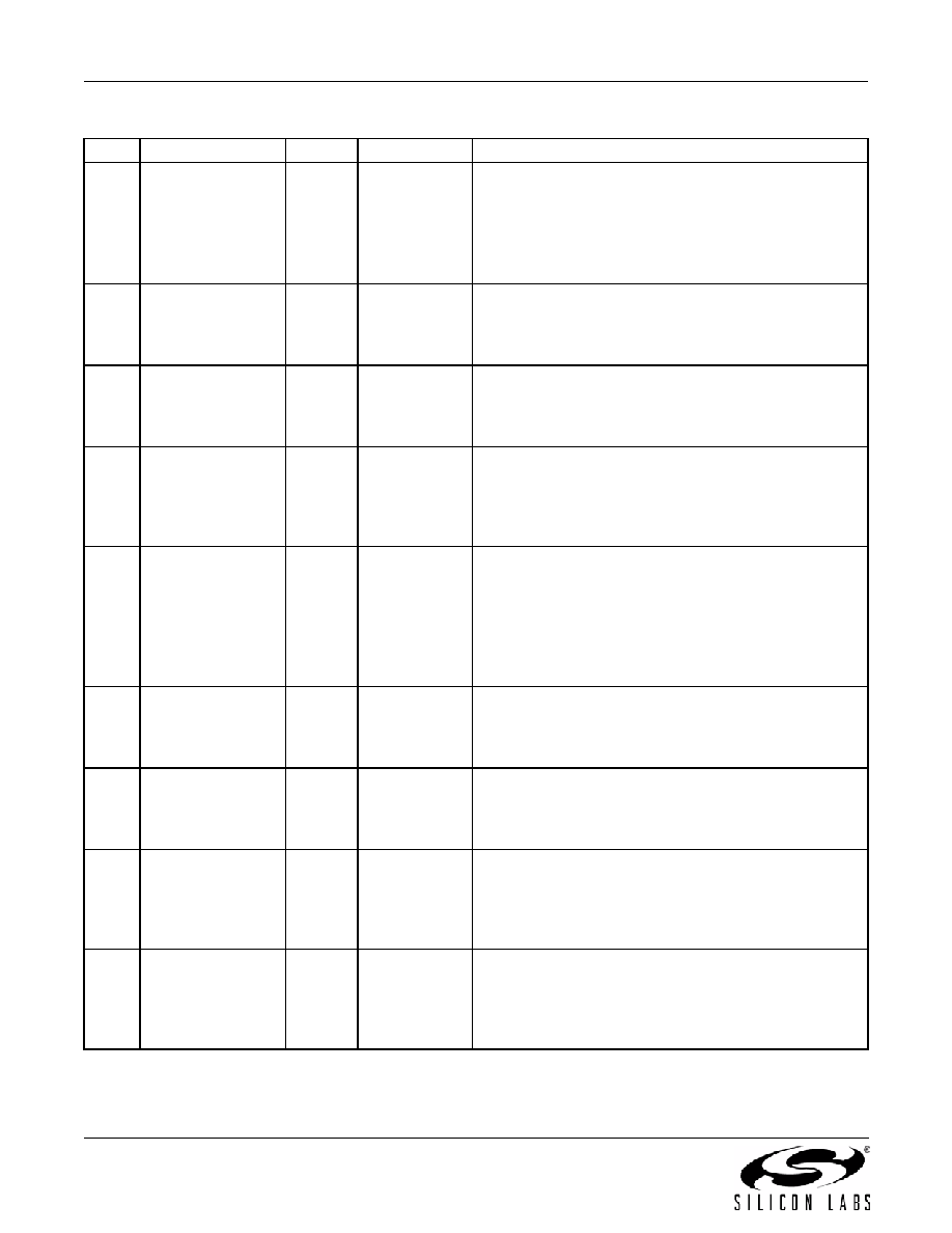
8
LOSLOL
O
Open Drain
Loss of Signal or Loss of Lock Indicator.
0 = No LOS or LOL condition.
1 = A LOS or LOL condition has occurred.
For this pin a 1–5 k
pull-up resistor to a voltage is
required. This voltage may be as high as 3.63 V
regardless of the voltage on pin 7.
9
CLK3B
O
Multi
Output Clock B for Channel 3
May be a single-ended output or half of a differential out-
put with CLK3A being the other differential half. If
unused leave this pin floating.
10
CLK3A
O
Multi
Output Clock A for Channel 3
May be a single-ended output or half of a differential
output with CLK3B being the other differential half. If
unused leave this pin floating.
11
VDDO3
VDD
Supply
Output Clock Supply Voltage
Supply voltage (3.3, 2.5, 1.8, or 1.5 V) for CLK3A,B. A
0.1 F capacitor must be located very close to this pin. If
CLK3 is not used, this pin must be tied to VDD (pin 7,
24).
12
IN7
I
Supply
SSPB.
When low, Spread Spectrum is enabled on every output
clock that is programmed for Spread Spectrum. This
option is available on the Si5334K/L/M.
On an Si5334 that does not contain the spread spectrum
functionality, this pin should be connected to GND.
13
CLK2B
O
Multi
Output Clock B for Channel 2
May be a single-ended output or half of a differential
output with CLK2A being the other differential half. If
unused leave this pin floating.
14
CLK2A
O
Multi
Output Clock A for Channel 2
May be a single-ended output or half of a differential
output with CLK2B being the other differential half. If
unused leave this pin floating.
15
VDDO2
VDD
Supply
Output Clock Supply Voltage.
Supply voltage (3.3, 2.5, 1.8, or 1.5 V) for CLK2A,B.
A 0.1 F capacitor must be located very close to this pin.
If CLK2 is not used, this pin must be tied to VDD (pin 7,
24).
16
VDDO1
VDD
Supply
Output Clock Supply Voltage.
Supply voltage (3.3, 2.5, 1.8, or 1.5 V) for CLK1A,B.
A 0.1 F capacitor must be located very close to this pin.
If CLK1 is not used, this pin must be tied to VDD (pin 7,
24).
Table 15. Si5334 Pin Descriptions (Continued)
Pin #
Pin Name
I/O
Signal Type
Description
相关PDF资料 |
PDF描述 |
|---|---|
| SI5334C-A00131-GMR | PLL BASED CLOCK DRIVER, QCC24 |
| SI5334C-A00135-GMR | PLL BASED CLOCK DRIVER, QCC24 |
| SI5334C-A00148-GMR | PLL BASED CLOCK DRIVER, QCC24 |
| SI5334C-A00150-GMR | PLL BASED CLOCK DRIVER, QCC24 |
| SI5334C-A00152-GM | PLL BASED CLOCK DRIVER, QCC24 |
相关代理商/技术参数 |
参数描述 |
|---|---|
| SI5334B-A00154-GM | 制造商:Silicon Laboratories Inc 功能描述:CLOCK - Rail/Tube |
| SI5334B-A00154-GMR | 制造商:Silicon Laboratories Inc 功能描述:CLOCK - Tape and Reel |
| SI5334B-A00156-GM | 制造商:Silicon Laboratories Inc 功能描述:CLOCK - Rail/Tube |
| SI5334B-A00156-GMR | 制造商:Silicon Laboratories Inc 功能描述:CLOCK - Tape and Reel |
| SI5334B-A00164-GM | 制造商:Silicon Laboratories Inc 功能描述:CLOCK - Rail/Tube |
发布紧急采购,3分钟左右您将得到回复。