- 您现在的位置:买卖IC网 > PDF目录8973 > SI5338E-A-GM (Silicon Laboratories Inc)IC CLK GEN I2C BUS PROG 24QFN PDF资料下载
参数资料
| 型号: | SI5338E-A-GM |
| 厂商: | Silicon Laboratories Inc |
| 文件页数: | 13/44页 |
| 文件大小: | 0K |
| 描述: | IC CLK GEN I2C BUS PROG 24QFN |
| 标准包装: | 490 |
| 系列: | MultiSynth™ |
| 类型: | * |
| PLL: | 是 |
| 输入: | CML,HCSL,HSCL,LVDS,LVPECL,晶体 |
| 输出: | CMOS,HCSL. HSTL. LVDS. LVPECL. SSTL |
| 电路数: | 1 |
| 比率 - 输入:输出: | 1:4 |
| 差分 - 输入:输出: | 是/是 |
| 频率 - 最大: | 350MHz |
| 除法器/乘法器: | 是/是 |
| 电源电压: | 1.71 V ~ 3.63 V |
| 工作温度: | -40°C ~ 85°C |
| 安装类型: | 表面贴装 |
| 封装/外壳: | 24-VFQFN 裸露焊盘 |
| 供应商设备封装: | 24-QFN(4x4) |
| 包装: | 托盘 |
第1页第2页第3页第4页第5页第6页第7页第8页第9页第10页第11页第12页当前第13页第14页第15页第16页第17页第18页第19页第20页第21页第22页第23页第24页第25页第26页第27页第28页第29页第30页第31页第32页第33页第34页第35页第36页第37页第38页第39页第40页第41页第42页第43页第44页
Si5338
20
Rev. 1.3
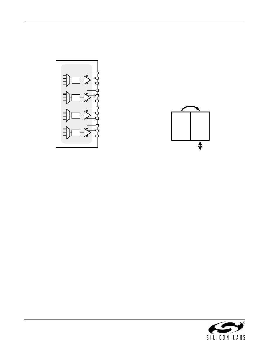
3.4. Output Stage
The output stage consists of output selectors, output
dividers, and programmable output drivers as shown in
Figure 7. Output Stage
The output selectors select the clock source for the
output drivers. By default, each output driver is
connected to its own MultiSynth block (e.g. MS0 to
CLK0, MS1 to CLK1, etc), but other combinations are
possible by reconfiguring the device. The PLL can be
bypassed by connecting the input stage signals (osc,
ref, refdiv, fb, or fbdiv) directly to the output divider.
Bypassing an input directly to an output will not allow
phase alignment of that output to other outputs. Each of
the output drivers can also connect to the first
MultiSynth block (MS0) enabling a fan-out function. This
allows the Si5338 to act as a clock generator, a fanout
buffer, or a combination of both in the same package.
The output dividers (R0, R1, R2, R3) allow another
stage of clock division.These dividers are configurable
as divide by 1 (default), 2, 4, 8, 16, or 32. When an Rn
does not equal 1, the phase alignment function for that
output will not work.
The output drivers are configurable to support common
signal formats, such as LVPECL, LVDS, HCSL, CMOS,
HSTL, and SSTL. Separate output supply pins (VDDOn)
are provided for each output buffer.
The voltage on these supply pins can be 3.3, 2.5, 1.8, or
1.5 V as needed for the possible output formats.
Additionally, the outputs can be configured to stop high,
low, or tri-state when the PLL has lost lock. If the Si5338
is used in a zero delay mode, the output that is fed back
must be set for always on, which will override any
output disable signal.
Each of the outputs can also be enabled or disabled
through the I2C port. A single pin to enable/disable all
outputs is available in the Si5338K/L/M.
3.5. Configuring the Si5338
The Si5338 is a highly-flexible clock generator that is
entirely configurable through its I2C interface. The
device’s default configuration is stored in non-volatile
memory (NVM) as shown in Figure 8. The NVM is a
one-time programmable memory (OTP), which can
store a custom user configuration at power-up. This is a
useful feature for applications that need a clock present
at power-up (e.g., for providing a clock to a processor).
Figure 8. Si5338 Memory Configuration
During a power cycle or a power-on reset (POR), the
contents of the NVM are copied into random access
memory (RAM), which sets the device configuration that
will be used during operation. Any changes to the
device configuration after power-up are made by
reading and writing to registers in the RAM space
through the I2C interface. ClockBuilder Desktop (see
can be used to easily configure register map files that
can be written into RAM (see “3.5.2. Creating a New
Configuration for RAM” for details). Alternatively, the
register map file can be created manually with the help
of the equations in the Si5338 Reference Manual.
Two versions of the Si5338 are available. First,
standard, non-customized Si5338 devices are available
in which the RAM can be configured in-circuit via I2C
(example part number Si5338C-A-GM). Alternatively,
standard Si5338 devices can be field-programmed
using the Si5338/56-PROG-EVB field programmer.
Second, custom factory-programmed Si5338 devices
are available that include a user-specified startup
frequency
configuration
(example
part
number
Si5338C-Axxxxx-GM). See "12. Ordering Information"
on page 41 for details.
CLK0A
VDDO1
VDDO2
VDDO3
VDDO0
CLK0B
CLK1A
CLK1B
CLK2A
CLK2B
CLK3A
CLK3B
÷R1
÷R0
÷R2
÷R3
Output
Stage
F
rom
Sy
nt
h
e
s
is
St
ag
e
or
Inpu
t
S
ta
g
e
Power-Up/POR
I
2C
RAM
NVM
(OTP)
Default
Config
相关PDF资料 |
PDF描述 |
|---|---|
| JN1KS10PL2 | CONN RCPT 10POS W/O PIN WALL MT |
| MS27468E17A55S | CONN RCPT 55POS JAM NUT W/SCKT |
| VE-JTY-MZ-F1 | CONVERTER MOD DC/DC 3.3V 16.5W |
| MS27474T22A2S | CONN RCPT 85POS JAM NUT W/SCKT |
| VE-JTX-MZ-F4 | CONVERTER MOD DC/DC 5.2V 25W |
相关代理商/技术参数 |
参数描述 |
|---|---|
| SI5338E-A-GMR | 功能描述:时钟发生器及支持产品 I2C-Program Clk Gen 0.16-350MHz Pin-Ctrl RoHS:否 制造商:Silicon Labs 类型:Clock Generators 最大输入频率:14.318 MHz 最大输出频率:166 MHz 输出端数量:16 占空比 - 最大:55 % 工作电源电压:3.3 V 工作电源电流:1 mA 最大工作温度:+ 85 C 安装风格:SMD/SMT 封装 / 箱体:QFN-56 |
| Si5338E-B-GM | 功能描述:时钟发生器及支持产品 I2C-PRGRMBL clock generatr 0.16-350MHz RoHS:否 制造商:Silicon Labs 类型:Clock Generators 最大输入频率:14.318 MHz 最大输出频率:166 MHz 输出端数量:16 占空比 - 最大:55 % 工作电源电压:3.3 V 工作电源电流:1 mA 最大工作温度:+ 85 C 安装风格:SMD/SMT 封装 / 箱体:QFN-56 |
| Si5338E-B-GMR | 功能描述:时钟发生器及支持产品 I2C-Program Clk Gen 0.16-350MHz Pin-Ctrl RoHS:否 制造商:Silicon Labs 类型:Clock Generators 最大输入频率:14.318 MHz 最大输出频率:166 MHz 输出端数量:16 占空比 - 最大:55 % 工作电源电压:3.3 V 工作电源电流:1 mA 最大工作温度:+ 85 C 安装风格:SMD/SMT 封装 / 箱体:QFN-56 |
| Si5338-EVB | 功能描述:时钟和定时器开发工具 Si5338/4/0 eval board RoHS:否 制造商:Texas Instruments 产品:Evaluation Modules 类型:Clock Conditioners 工具用于评估:LMK04100B 频率:122.8 MHz 工作电源电压:3.3 V |
| SI5338F-A01839-GM | 制造商:Silicon Laboratories Inc 功能描述:CLOCK - Bulk |
发布紧急采购,3分钟左右您将得到回复。