- 您现在的位置:买卖IC网 > PDF目录8973 > SI5338E-A-GM (Silicon Laboratories Inc)IC CLK GEN I2C BUS PROG 24QFN PDF资料下载
参数资料
| 型号: | SI5338E-A-GM |
| 厂商: | Silicon Laboratories Inc |
| 文件页数: | 29/44页 |
| 文件大小: | 0K |
| 描述: | IC CLK GEN I2C BUS PROG 24QFN |
| 标准包装: | 490 |
| 系列: | MultiSynth™ |
| 类型: | * |
| PLL: | 是 |
| 输入: | CML,HCSL,HSCL,LVDS,LVPECL,晶体 |
| 输出: | CMOS,HCSL. HSTL. LVDS. LVPECL. SSTL |
| 电路数: | 1 |
| 比率 - 输入:输出: | 1:4 |
| 差分 - 输入:输出: | 是/是 |
| 频率 - 最大: | 350MHz |
| 除法器/乘法器: | 是/是 |
| 电源电压: | 1.71 V ~ 3.63 V |
| 工作温度: | -40°C ~ 85°C |
| 安装类型: | 表面贴装 |
| 封装/外壳: | 24-VFQFN 裸露焊盘 |
| 供应商设备封装: | 24-QFN(4x4) |
| 包装: | 托盘 |
第1页第2页第3页第4页第5页第6页第7页第8页第9页第10页第11页第12页第13页第14页第15页第16页第17页第18页第19页第20页第21页第22页第23页第24页第25页第26页第27页第28页当前第29页第30页第31页第32页第33页第34页第35页第36页第37页第38页第39页第40页第41页第42页第43页第44页
Si5338
Rev. 1.3
35
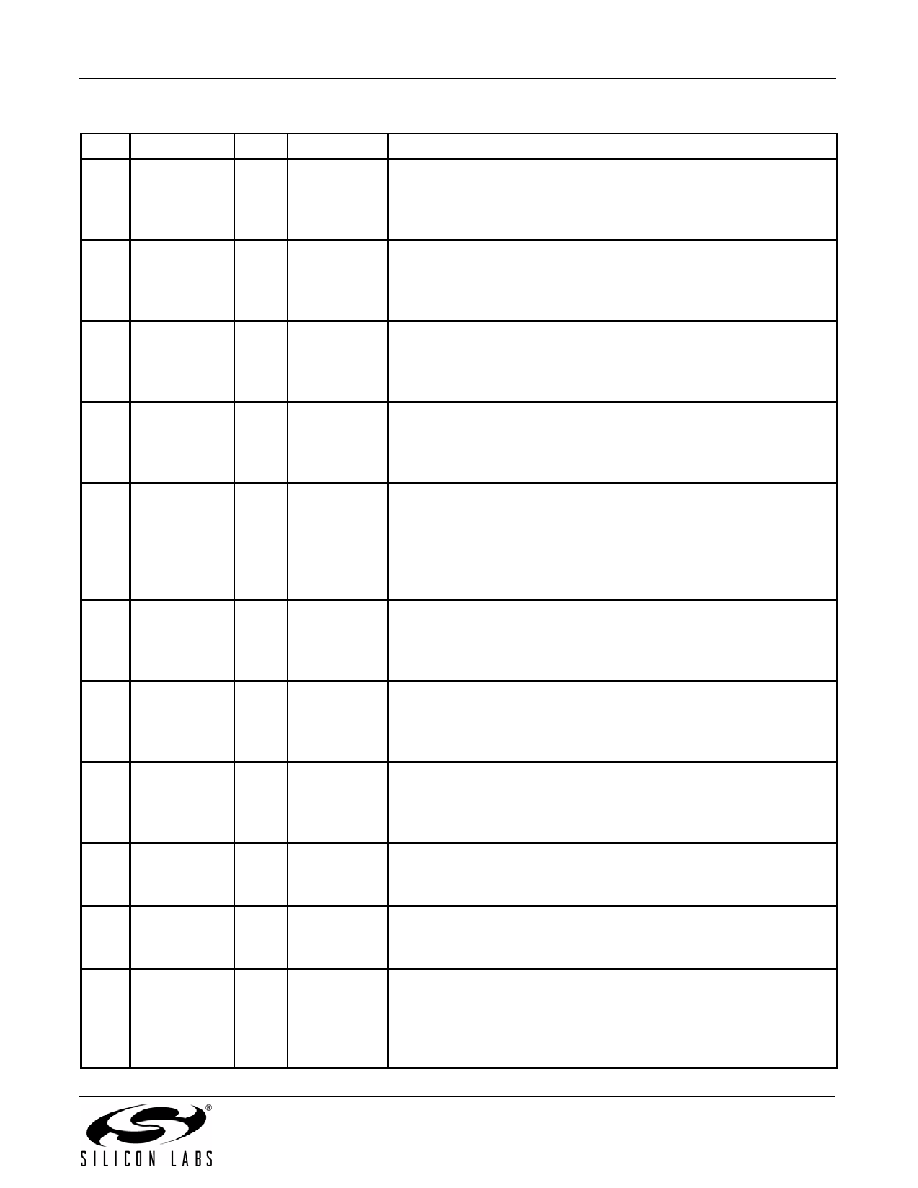
15
VDDO2
VDD
Supply
Output Clock Supply Voltage.
Supply voltage (3.3, 2.5, 1.8, or 1.5 V) for CLK2A,B.
A 0.1 F capacitor must be located very close to this pin. If CLK2 is
not used, this pin must be tied to VDD (pin 7, 24).
16
VDDO1
VDD
Supply
Output Clock Supply Voltage.
Supply voltage (3.3, 2.5, 1.8, or 1.5 V) for CLK1A,B.
A 0.1 F capacitor must be located very close to this pin. If CLK1 is
not used, this pin must be tied to VDD (pin 7, 24).
17
CLK1B
O
Multi
Output Clock B for Channel 1.
May be a single-ended output or half of a differential output with
CLK1A being the other differential half. If unused, leave this pin
floating.
18
CLK1A
O
Multi
Output Clock A for Channel 1.
May be a single-ended output or half of a differential output with
CLK1B being the other differential half. If unused, leave this pin
floating.
19
SDA
I/O
LVCMOS
I2C Serial Data.
This is the serial data for the I2C bus. A pullup resistor at this pin is
required. Typical values would be 1–4 k
. See the I2C bus spec
for more information. This pin is 3.3 V tolerant regardless of the
other supply voltages on pins 7, 11, 15, 16, 20, 24. See Register
27.
20
VDDO0
VDD
Supply
Output Clock Supply Voltage.
Supply voltage (3.3, 2.5, 1.8, or 1.5 V) for CLK0A,B.
A 0.1 F capacitor must be located very close to this pin. If CLK0 is
not used, this pin must be tied to VDD (pin 7, 24).
21
CLK0B
O
Multi
Output Clock B for Channel 0.
May be a single-ended output or half of a differential output with
CLK0A being the other differential half. If unused, leave this pin
floating.
22
CLK0A
O
Multi
Output Clock A for Channel 0.
May be a single-ended output or half of a differential output with
CLK0B being the other differential half. If unused, leave this pin
floating.
23
RSVD_GND
GND
Ground.
Must be connected to system ground. Minimize the ground path
impedance for optimal performance of this device.
24
VDD
Supply
Core Supply Voltage.
The device operates from a 1.8, 2.5, or 3.3 V supply. A 0.1 F
bypass capacitor should be located very close to this pin.
GND
PAD
GND
Ground Pad.
This is the large pad in the center of the package. Device
specifications cannot be guaranteed unless the ground pad is
properly connected to a ground plane on the PCB. See Table 19,
“PCB Land Pattern,” on page 39 for ground via requirements.
Table 16. Si5338 Pin Descriptions (Continued)
Pin #
Pin Name
I/O
Signal Type
Description
相关PDF资料 |
PDF描述 |
|---|---|
| JN1KS10PL2 | CONN RCPT 10POS W/O PIN WALL MT |
| MS27468E17A55S | CONN RCPT 55POS JAM NUT W/SCKT |
| VE-JTY-MZ-F1 | CONVERTER MOD DC/DC 3.3V 16.5W |
| MS27474T22A2S | CONN RCPT 85POS JAM NUT W/SCKT |
| VE-JTX-MZ-F4 | CONVERTER MOD DC/DC 5.2V 25W |
相关代理商/技术参数 |
参数描述 |
|---|---|
| SI5338E-A-GMR | 功能描述:时钟发生器及支持产品 I2C-Program Clk Gen 0.16-350MHz Pin-Ctrl RoHS:否 制造商:Silicon Labs 类型:Clock Generators 最大输入频率:14.318 MHz 最大输出频率:166 MHz 输出端数量:16 占空比 - 最大:55 % 工作电源电压:3.3 V 工作电源电流:1 mA 最大工作温度:+ 85 C 安装风格:SMD/SMT 封装 / 箱体:QFN-56 |
| Si5338E-B-GM | 功能描述:时钟发生器及支持产品 I2C-PRGRMBL clock generatr 0.16-350MHz RoHS:否 制造商:Silicon Labs 类型:Clock Generators 最大输入频率:14.318 MHz 最大输出频率:166 MHz 输出端数量:16 占空比 - 最大:55 % 工作电源电压:3.3 V 工作电源电流:1 mA 最大工作温度:+ 85 C 安装风格:SMD/SMT 封装 / 箱体:QFN-56 |
| Si5338E-B-GMR | 功能描述:时钟发生器及支持产品 I2C-Program Clk Gen 0.16-350MHz Pin-Ctrl RoHS:否 制造商:Silicon Labs 类型:Clock Generators 最大输入频率:14.318 MHz 最大输出频率:166 MHz 输出端数量:16 占空比 - 最大:55 % 工作电源电压:3.3 V 工作电源电流:1 mA 最大工作温度:+ 85 C 安装风格:SMD/SMT 封装 / 箱体:QFN-56 |
| Si5338-EVB | 功能描述:时钟和定时器开发工具 Si5338/4/0 eval board RoHS:否 制造商:Texas Instruments 产品:Evaluation Modules 类型:Clock Conditioners 工具用于评估:LMK04100B 频率:122.8 MHz 工作电源电压:3.3 V |
| SI5338F-A01839-GM | 制造商:Silicon Laboratories Inc 功能描述:CLOCK - Bulk |
发布紧急采购,3分钟左右您将得到回复。