- 您现在的位置:买卖IC网 > PDF目录8964 > SI5367A-C-GQR (Silicon Laboratories Inc)IC CLOCK MULTIPLIER PROG 100TQFP PDF资料下载
参数资料
| 型号: | SI5367A-C-GQR |
| 厂商: | Silicon Laboratories Inc |
| 文件页数: | 68/80页 |
| 文件大小: | 0K |
| 描述: | IC CLOCK MULTIPLIER PROG 100TQFP |
| 标准包装: | 250 |
| 系列: | DSPLL® |
| 类型: | 时钟乘法器 |
| PLL: | 是 |
| 输入: | 时钟 |
| 输出: | CML,CMOS,LVDS,LVPECL |
| 电路数: | 1 |
| 比率 - 输入:输出: | 4:5 |
| 差分 - 输入:输出: | 是/是 |
| 频率 - 最大: | 1.42GHz |
| 除法器/乘法器: | 无/是 |
| 电源电压: | 1.71 V ~ 2.75 V |
| 工作温度: | -40°C ~ 85°C |
| 安装类型: | 表面贴装 |
| 封装/外壳: | 100-TQFP |
| 供应商设备封装: | 100-TQFP(14x14) |
| 包装: | 带卷 (TR) |
第1页第2页第3页第4页第5页第6页第7页第8页第9页第10页第11页第12页第13页第14页第15页第16页第17页第18页第19页第20页第21页第22页第23页第24页第25页第26页第27页第28页第29页第30页第31页第32页第33页第34页第35页第36页第37页第38页第39页第40页第41页第42页第43页第44页第45页第46页第47页第48页第49页第50页第51页第52页第53页第54页第55页第56页第57页第58页第59页第60页第61页第62页第63页第64页第65页第66页第67页当前第68页第69页第70页第71页第72页第73页第74页第75页第76页第77页第78页第79页第80页
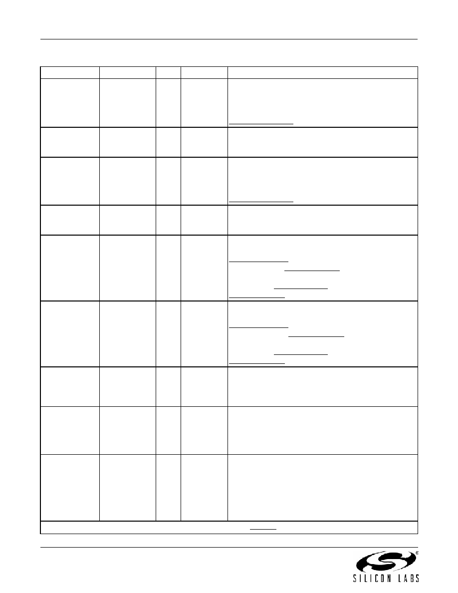
Si5367
70
Rev. 0.5
29
30
CKIN4+
CKIN4–
IMULTI
Clock Input 4.
Differential clock input. This input can also be driven with
a single-ended signal. CKIN4 serves as the frame sync
input associated with the CKIN2 clock when
CK_CONFIG_REG =1.
34
35
CKIN2+
CKIN2–
IMULTI
Clock Input 2.
Differential input clock. This input can also be driven with
a single-ended signal.
39
40
CKIN3+
CKIN3–
IMULTI
Clock Input 3.
Differential clock input. This input can also be driven with
a single-ended signal. CKIN3 serves as the frame sync
input associated with the CKIN1 clock when
CK_CONFIG_REG =1.
44
45
CKIN1+
CKIN1–
IMULTI
Clock Input 1.
Differential clock input. This input can also be driven with
a single-ended signal.
58
C1A
O
LVCMOS
CKIN1 Active Clock Indicator.
This pin serves as the CKIN1 active clock indicator. The
CK1_ACTV_REG bit always reflects the active clock sta-
tus for CKIN1. If CK1_ACTV_PIN = 1, this status will
also be reflected on the C1A pin with active polarity con-
trolled by the CK_ACTV_POL bit. If
CK1_ACTV_PIN = 0, this output tristates.
59
C2A
O
LVCMOS
CKIN2 Active Clock Indicator.
This pin serves as the CKIN2 active clock indicator. The
CK2_ACTV_REG bit always reflects the active clock sta-
tus for CKIN_2. If CK2_ACTV_PIN = 1, this status will
also be reflected on the C2A pin with active polarity con-
trolled by the CK_ACTV_POL bit. If
CK2_ACTV_PIN = 0, this output tristates.
60
SCL
I
LVCMOS
Serial Clock.
This pin functions as the serial port clock input for both
SPI and I2C modes.
This pin has a weak pull-down.
61
SDA_SDO
I/O
LVCMOS
Serial Data.
In I2C microprocessor control mode (CMODE = 0), this
pin functions as the bidirectional serial data port.In SPI
microprocessor control mode (CMODE = 1), this pin
functions as the serial data output.
68
69
A0
A1
ILVCMOS
Serial Port Address.
In I2C control mode (CMODE = 0), these pins function as
hardware controlled address bits. The I2C address is
1101 [A2][A1][A0.]
In SPI control mode (CMODE = 1), these pins are
ignored.
This pin has a weak pull-down.
Table 11. Si5367 Pin Descriptions (Continued)
Pin #
Pin Name
I/O
Signal Level
Description
Note: Internal register names are indicated by underlined italics, e.g. INT_PIN. See Si5368 Register Map.
相关PDF资料 |
PDF描述 |
|---|---|
| AD5754RBREZ | IC DAC 16BIT DSP/SRL 24TSSOP |
| VI-JTX-MZ-F1 | CONVERTER MOD DC/DC 5.2V 25W |
| LTC1650CS#PBF | IC D/A CONV 16BIT R-R 16-SOIC |
| VI-JTW-MZ-F3 | CONVERTER MOD DC/DC 5.5V 25W |
| VI-JTW-MZ-F4 | CONVERTER MOD DC/DC 5.5V 25W |
相关代理商/技术参数 |
参数描述 |
|---|---|
| Si5367B-B-GQ | 功能描述:时钟合成器/抖动清除器 uP-PROGRAMMABE CLK MULT 10 MHZ-808 MHZ RoHS:否 制造商:Skyworks Solutions, Inc. 输出端数量: 输出电平: 最大输出频率: 输入电平: 最大输入频率:6.1 GHz 电源电压-最大:3.3 V 电源电压-最小:2.7 V 封装 / 箱体:TSSOP-28 封装:Reel |
| SI5367B-B-GQR | 制造商:Silicon Laboratories Inc 功能描述: |
| Si5367B-C-GQ | 功能描述:时钟合成器/抖动清除器 uP-PROGRAMMABE CLK MULT 10 MHZ-808 MHZ RoHS:否 制造商:Skyworks Solutions, Inc. 输出端数量: 输出电平: 最大输出频率: 输入电平: 最大输入频率:6.1 GHz 电源电压-最大:3.3 V 电源电压-最小:2.7 V 封装 / 箱体:TSSOP-28 封装:Reel |
| SI5367B-C-GQR | 功能描述:时钟发生器及支持产品 mP-Program Precision Clk Multiplier 4/5 RoHS:否 制造商:Silicon Labs 类型:Clock Generators 最大输入频率:14.318 MHz 最大输出频率:166 MHz 输出端数量:16 占空比 - 最大:55 % 工作电源电压:3.3 V 工作电源电流:1 mA 最大工作温度:+ 85 C 安装风格:SMD/SMT 封装 / 箱体:QFN-56 |
| Si5367C-B-GQ | 功能描述:时钟合成器/抖动清除器 uP-PROGRAMMABE CLK MULT 10 MHZ-346 MHZ RoHS:否 制造商:Skyworks Solutions, Inc. 输出端数量: 输出电平: 最大输出频率: 输入电平: 最大输入频率:6.1 GHz 电源电压-最大:3.3 V 电源电压-最小:2.7 V 封装 / 箱体:TSSOP-28 封装:Reel |
发布紧急采购,3分钟左右您将得到回复。