- 您现在的位置:买卖IC网 > PDF目录13093 > SI9130CG-E3 (Vishay Siliconix)IC CTRLR PWM PIN PROG 28SSOP PDF资料下载
参数资料
| 型号: | SI9130CG-E3 |
| 厂商: | Vishay Siliconix |
| 文件页数: | 11/15页 |
| 文件大小: | 0K |
| 描述: | IC CTRLR PWM PIN PROG 28SSOP |
| 标准包装: | 225 |
| 应用: | 控制器,移动式个人电脑 |
| 输入电压: | 5.5 V ~ 30 V |
| 输出数: | 2 |
| 输出电压: | 5V,可编程 |
| 工作温度: | 0°C ~ 70°C |
| 安装类型: | 表面贴装 |
| 封装/外壳: | 28-SSOP(0.209",5.30mm 宽) |
| 供应商设备封装: | 28-SSOP |
| 包装: | 散装 |
�� �
�
�Product� is� End� of� Life� 3/2014�
�Si9130�
�Vishay� Siliconix�
�cycle� in� continuous� mode,� or� until� the� inductor� current�
�becomes� positive� again,� in� discontinuous� mode.� In� over-�
�current� situations,� where� the� inductor� current� is� greater� than�
�the� 100� mV� current-limit� threshold,� the� high-side� latch� is�
�reset� and� the� high-side� gate� drive� is� shut� off.�
�During� low-current� load� requirements,� the� inductor� current�
�will� not� deliver� the� 25� mV� minimum� current� threshold.� The�
�Minimum� Current� comparator� signals� the� PWM� to� enter�
�pulse-skipping� mode� when� the� threshold� has� not� been�
�reached.� pulse-skipping� mode� skips� pulses� to� reduce�
�switching� losses,� the� losses� which� decrease� efficiency� the�
�most� at� light� load.� Entering� this� mode� causes� the� minimum�
�current� comparator� to� reset� the� high-side� latch� at� the�
�beginning� of� each� oscillator� cycle.�
�Soft-Start�
�To� slowly� bring� up� the� 3.3� V� and� 5� V� supplies,� connect�
�capacitors� from� SS� 3� and� SS� 5� to� GND.� Asserting� ON� 3� or� ON� 5�
�starts� a� 4� A� constant� current� source� to� charge� these�
�capacitors� to� 4� V.� As� the� voltage� on� these� pins� ramps� up,� so�
�does� the� current� limit� comparator� threshold,� to� increase� the�
�duty� cycle� of� the� MOSFETs� to� their� maximum� level.� If� ON� 3� or�
�ON� 5� are� left� low,� the� respective� capacitor� is� discharged� to�
�GND.� Leaving� the� SS� 3� or� SS� 5� pins� open� will� cause� either�
�controller� to� reach� the� terminal� over-current� level� within�
�10� μs.�
�Soft� start� helps� prevent� current� spikes� at� turn-on� and� allows�
�separate� supplies� to� be� delayed� using� external�
�Synchronous� rectification� is� always� active� when� the� Si9130�
�is� powered-up,� regardless� of� the� operational� mode.�
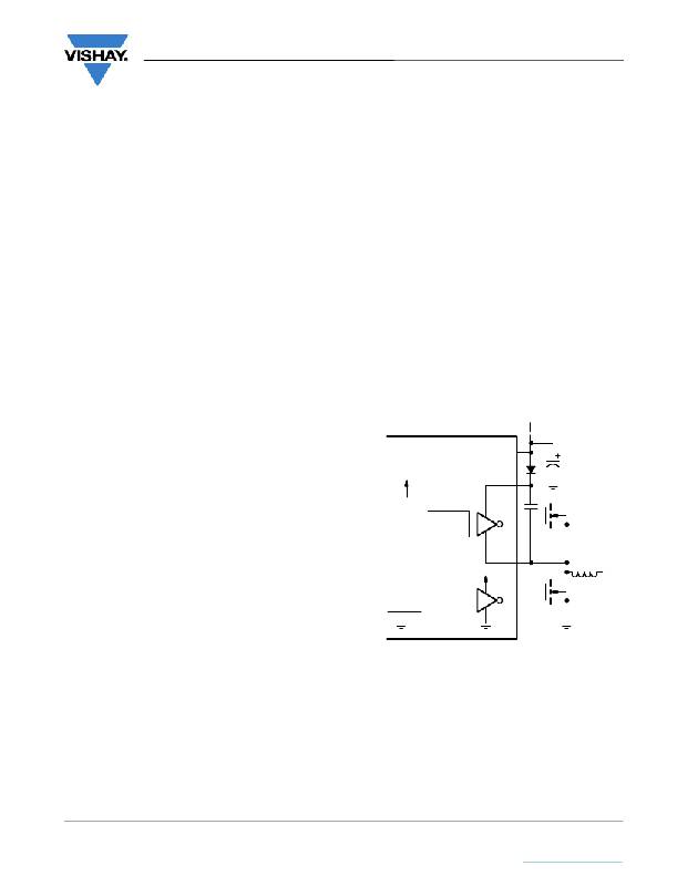
�Gate-Driver� Boost�
�The� high-side� N-Channel� drive� is� supplied� by� a� flying-�
�capacitor� boost� circuit� (see� Figure� 4).� The� capacitor� takes� a�
�charge� from� V� L� and� then� is� connected� from� gate� to� source� of�
�the� high-side� MOSFET� to� provide� gate� enhancement.� At�
�power-up,� the� low-side� MOSFET� pulls� LX_� down� to� GND�
�and� charges� the� BST_� capacitor� connected� to� 5� V.� During�
�the� second� half� of� the� oscillator� cycle,� the� controller� drives�
�the� gate� of� the� high-side� MOSFET� by� internally� connecting�
�node� BST_� to� DH_.� This� supplies� a� voltage� 5� V� higher� than�
�the� battery� voltage� to� the� gate� of� the� high-side� MOSFET.�
�Oscillations� on� the� gates� of� the� high-side� MOSFET� in�
�discontinuous� mode� are� a� natural� occurrence� caused� by� the�
�LC� network� formed� by� the� inductor� and� stray� capacitance� at�
�the� LX_� pins.� The� negative� side� of� the� BST_� capacitor� is�
�connected� to� the� LX_� node,� so� ringing� at� the� inductor� is�
�translated� through� to� the� gate� drive.�
�BATTERY�
�INPUT�
�V� L�
�programmability.�
�Synchronous� Rectifiers�
�Synchronous� rectification� replaces� the� Schottky� rectifier� with�
�a� MOSFET,� which� can� be� controlled� to� increase� the�
�efficiency� of� the� circuit.�
�When� the� high-side� MOSFET� is� switched� off,� the� inductor� will�
�try� to� maintain� its� current� flow,� inverting� the� inductor’s�
�polarity.� The� path� of� current� then� becomes� the� circuit� made�
�of� the� Schottky� diode,� inductor� and� load,� which� will� charge�
�the� output� capacitor.� The� diode� has� a� 0.5� V� forward� voltage�
�drop,� which� contributes� a� significant� amount� of� power� loss,�
�decreasing� efficiency.� A� low-side� switch� is� placed� in� parallel�
�with� the� Schottky� diode� and� is� turned� on� just� after� the� diode�
�V� L�
�PWM�
�Level�
�Translator�
�BST_�
�DH_�
�LX_�
�V� L�
�DL_�
�begins� to� conduct.� Because� the� r� DS(ON)� of� the� MOSFET� is�
�low,� the� I*R� voltage� drop� will� not� be� as� large� as� the� diode,�
�which� increases� efficiency.�
�The� low-side� rectifier� is� shut� off� when� the� inductor� current�
�drops� to� zero.�
�Shoot-through� current� is� the� result� when� both� the� high-side�
�and� rectifying� MOSFETs� are� turned� on� at� the� same� time.�
�Break-before-make� timing� internal� to� the� Si9130� manages�
�this� potential� problem.� During� the� time� when� neither�
�MOSFET� is� on,� the� Schottky� is� conducting,� so� that� the� body�
�diode� in� the� low-side� MOSFET� is� not� forced� to� conduct.�
�Document� Number:� 70190�
�S11-0975-Rev.� G,� 16-May-11�
�Figure� 4.� Boost� Supply� for� Gate� Drivers�
�www.vishay.com�
�11�
�This� document� is� subject� to� change� without� notice.�
�THE� PRODUCTS� DESCRIBED� HEREIN� AND� THIS� DOCUMENT� ARE� SUBJECT� TO� SPECIFIC� DISCLAIMERS,� SET� FORTH� AT� www.vishay.com/doc?91000�
�相关PDF资料 |
PDF描述 |
|---|---|
| VE-J5M-CZ-B1 | CONVERTER MOD DC/DC 10V 25W |
| VI-B54-EU-F1 | CONVERTER MOD DC/DC 48V 200W |
| VI-J1F-EZ-B1 | CONVERTER MOD DC/DC 72V 25W |
| C0603X7R1A103M | CAP CER 10000PF 10V 20% X7R 0201 |
| VE-J51-CZ-B1 | CONVERTER MOD DC/DC 12V 25W |
相关代理商/技术参数 |
参数描述 |
|---|---|
| SI9130CG-T1 | 功能描述:电流型 PWM 控制器 Pin-Programmable Dual Controller RoHS:否 制造商:Texas Instruments 开关频率:27 KHz 上升时间: 下降时间: 工作电源电压:6 V to 15 V 工作电源电流:1.5 mA 输出端数量:1 最大工作温度:+ 105 C 安装风格:SMD/SMT 封装 / 箱体:TSSOP-14 |
| SI9130CG-T1-E3 | 功能描述:IC CTRLR PWM PIN PROG 28SSOP RoHS:是 类别:集成电路 (IC) >> PMIC - 稳压器 - 专用型 系列:- 标准包装:2,000 系列:- 应用:控制器,DSP 输入电压:4.5 V ~ 25 V 输出数:2 输出电压:最低可调至 1.2V 工作温度:-40°C ~ 85°C 安装类型:表面贴装 封装/外壳:30-TFSOP(0.173",4.40mm 宽) 供应商设备封装:30-TSSOP 包装:带卷 (TR) |
| SI9130DB | 功能描述:电流型 PWM 控制器 SI9130 Demo Board RoHS:否 制造商:Texas Instruments 开关频率:27 KHz 上升时间: 下降时间: 工作电源电压:6 V to 15 V 工作电源电流:1.5 mA 输出端数量:1 最大工作温度:+ 105 C 安装风格:SMD/SMT 封装 / 箱体:TSSOP-14 |
| SI9130LG | 功能描述:电流型 PWM 控制器 Prog Dual Controller RoHS:否 制造商:Texas Instruments 开关频率:27 KHz 上升时间: 下降时间: 工作电源电压:6 V to 15 V 工作电源电流:1.5 mA 输出端数量:1 最大工作温度:+ 105 C 安装风格:SMD/SMT 封装 / 箱体:TSSOP-14 |
| SI9130LG-E3 | 功能描述:电流型 PWM 控制器 Pin-Programmable Dual Controller RoHS:否 制造商:Texas Instruments 开关频率:27 KHz 上升时间: 下降时间: 工作电源电压:6 V to 15 V 工作电源电流:1.5 mA 输出端数量:1 最大工作温度:+ 105 C 安装风格:SMD/SMT 封装 / 箱体:TSSOP-14 |
发布紧急采购,3分钟左右您将得到回复。