- 您现在的位置:买卖IC网 > Datasheet目录516 > SIS412DN-T1-GE3 (Vishay Siliconix)MOSFET N-CH D-S 30V 1212-8 PPAK Datasheet资料下载
参数资料
| 型号: | SIS412DN-T1-GE3 |
| 厂商: | Vishay Siliconix |
| 文件页数: | 1/13页 |
| 文件大小: | 0K |
| 描述: | MOSFET N-CH D-S 30V 1212-8 PPAK |
| 标准包装: | 1 |
| 系列: | TrenchFET® |
| FET 型: | MOSFET N 通道,金属氧化物 |
| FET 特点: | 逻辑电平门 |
| 漏极至源极电压(Vdss): | 30V |
| 电流 - 连续漏极(Id) @ 25° C: | 12A |
| 开态Rds(最大)@ Id, Vgs @ 25° C: | 24 毫欧 @ 7.8A,10V |
| Id 时的 Vgs(th)(最大): | 2.5V @ 250µA |
| 闸电荷(Qg) @ Vgs: | 12nC @ 10V |
| 输入电容 (Ciss) @ Vds: | 435pF @ 15V |
| 功率 - 最大: | 15.6W |
| 安装类型: | 表面贴装 |
| 封装/外壳: | PowerPAK? 1212-8 |
| 供应商设备封装: | PowerPAK? 1212-8 |
| 包装: | 标准包装 |
| 其它名称: | SIS412DN-T1-GE3DKR |
�� �
�
�New� Product�
�SiS412DN�
�Vishay� Siliconix�
�N-Channel� 30-V� (D-S)� MOSFET�
�PRODUCT� SUMMARY�
�FEATURES�
�V� DS� (V)�
�30�
�R� DS(on)� (� Ω� )�
�0.024� at� V� GS� =� 10� V�
�0.030� at� V� GS� =� 4.5� V�
�I� D� (A)� a�
�12�
�12�
�Q� g� (Typ.)�
�3.8� nC�
�?� Halogen-free� According� to� IEC� 61249-2-21�
�?� TrenchFET� ?� Power� MOSFET�
�?� 100� %� R� g� Tested�
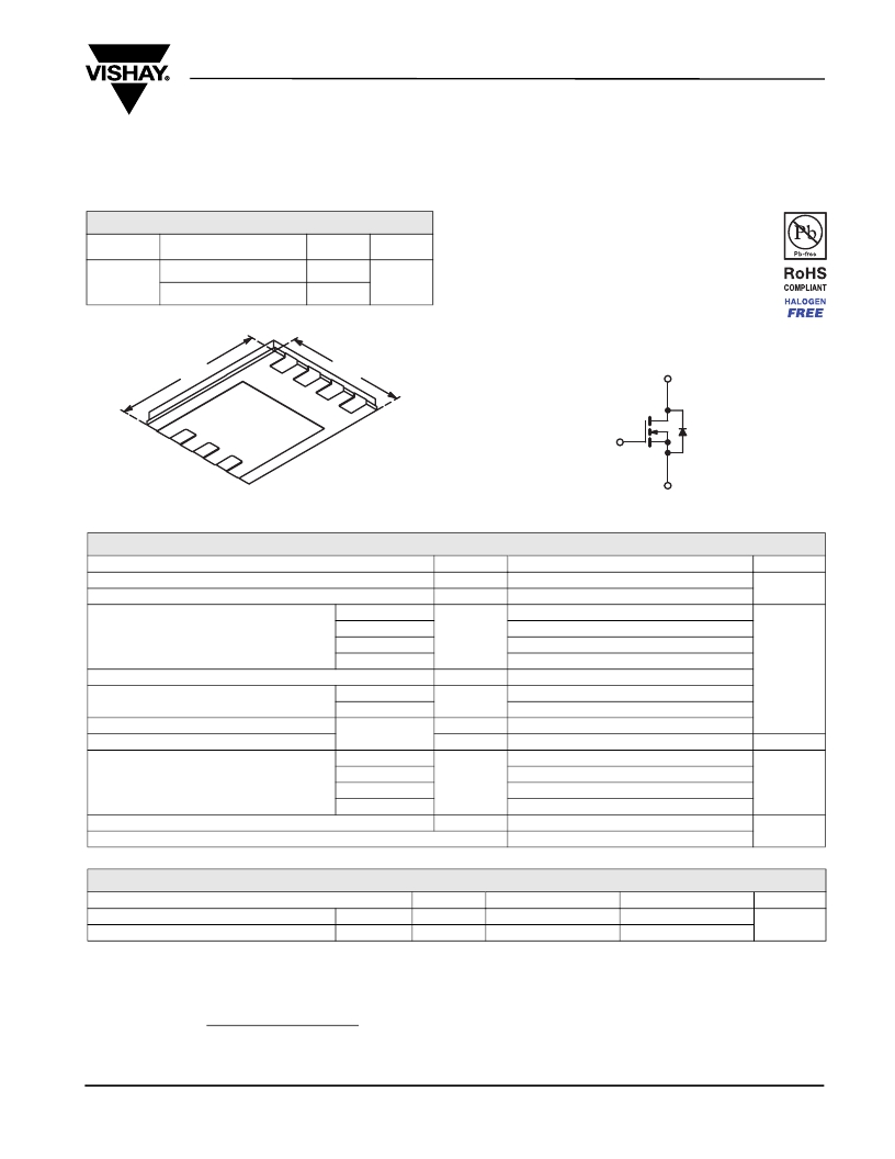
�PowerPAK� 1212-8�
�APPLICATIONS�
�?� Notebook� PC�
�-� System� Power�
�3.30� mm�
�1�
�S�
�S�
�3.30� mm�
�-� Load� Switch�
�D�
�2�
�3�
�S�
�G�
�4�
�D�
�8�
�7�
�D�
�6�
�D�
�5�
�D�
�G�
�Bottom� V� ie� w�
�Orderin� g� Information:� SiS412D� N� -T1-GE3� (Lead� (P� b� )-free� and� Halogen-free)�
�ABSOLUTE� MAXIMUM� RATINGS� T� A� =� 25� °C,� unless� otherwise� noted�
�S�
�N� -Channel� MOSFET�
�Parameter�
�Drain-Source� Voltage�
�Gate-Source� Voltage�
�T� C� =� 25� °C�
�Symbol�
�V� DS�
�V� GS�
�Limit�
�30�
�±� 20�
�12� a�
�Unit�
�V�
�Continuous� Drain� Current� (T� J� =� 150� °C)�
�T� C� =� 70� °C�
�T� A� =� 25� °C�
�I� D�
�12� a�
�8.7� b,� c�
�Pulsed� Drain� Current�
�Continuous� Source-Drain� Diode� Current�
�Single� Pulse� Avalanche� Current�
�Single� Pulse� Avalanche� Energy�
�T� A� =� 70� °C�
�T� C� =� 25� °C�
�T� A� =� 25� °C�
�L� =� 0.1� mH�
�I� DM�
�I� S�
�I� AS�
�E� AS�
�7� b,� c�
�30�
�12� a�
�2.7� b,� c�
�5�
�1.25�
�A�
�mJ�
�T� C� =� 25� °C�
�15.6�
�Maximum� Power� Dissipation�
�T� C� =� 70� °C�
�T� A� =� 25� °C�
�P� D�
�10�
�3.2� b,� c�
�W�
�T� A� =� 70� °C�
�2� b,� c�
�Operating� Junction� and� Storage� Temperature� Range�
�Soldering� Recommendations� (Peak� Temperature)� e,� f�
�T� J� ,� T� stg�
�-� 55� to� 150�
�260�
�°C�
�THERMAL� RESISTANCE� RATINGS�
�Parameter�
�Symbol�
�Typical�
�Maximum�
�Unit�
�Maximum� Junction-to-Ambient� b,� d�
�Maximum� Junction-to-Case� (Drain)�
�t� ≤� 10� s�
�Steady� State�
�R� thJA�
�R� thJC�
�32�
�6.5�
�39�
�8�
�°C/W�
�Notes:�
�a.� Package� Limited.�
�b.� Surface� Mounted� on� 1"� x� 1"� FR4� board.�
�c.� t� =� 10� s.�
�d.� Maximum� under� Steady� State� conditions� is� 81� °C/W.�
�e.� See� Solder� Profile� (� www.vishay.com/ppg?73257� ).� The� PowerPAK� 1212� is� a� leadless� package.� The� end� of� the� lead� terminal� is� exposed�
�copper� (not� plated)� as� a� result� of� the� singulation� process� in� manufacturing.� A� solder� fillet� at� the� exposed� copper� tip� cannot� be� guaranteed� and�
�is� not� required� to� ensure� adequate� bottom� side� solder� interconnection.�
�f.� Rework� Conditions:� manual� soldering� with� a� soldering� iron� is� not� recommended� for� leadless� components.�
�Document� Number:� 69006�
�S09-0135-Rev.� C,� 02-Feb-09�
�www.vishay.com�
�1�
�相关PDF资料 |
PDF描述 |
|---|---|
| SIS426DN-T1-GE3 | MOSFET N-CH 20V 35A 1212-8 |
| SIS436DN-T1-GE3 | MOSFET N-CH D-S 25V PPAK 1212-8 |
| SIS452DN-T1-GE3 | MOSFET N-CH D-S 12V 1212-8 PPAK |
| SIS456DN-T1-GE3 | MOSFET N-CH 30V 1212-8 PPAK |
| SIS468DN-T1-GE3 | MOSF N CH 80V 30A 1212-8 PWR PK |
相关代理商/技术参数 |
参数描述 |
|---|---|
| SIS413DN-T1-GE3 | 功能描述:MOSFET -30V 9.4mOhm@10V -18A P-Ch G-III RoHS:否 制造商:Vishay Semiconductors 晶体管极性:P-Channel 汲极/源极击穿电压:30 V 闸/源击穿电压:+/- 20 V 漏极连续电流:18 A 电阻汲极/源极 RDS(导通):9.4 mOhms 配置:Single 最大工作温度:+ 150 C 安装风格:SMD/SMT 封装 / 箱体:PowerPAK 1212-8 封装:Reel |
| SIS414DN | 制造商:VISHAY 制造商全称:Vishay Siliconix 功能描述:N-Channel 30 V (D-S) MOSFET |
| SIS414DN-T1-GE3 | 功能描述:MOSFET 20V 20A N-CH MOSFET RoHS:否 制造商:STMicroelectronics 晶体管极性:N-Channel 汲极/源极击穿电压:650 V 闸/源击穿电压:25 V 漏极连续电流:130 A 电阻汲极/源极 RDS(导通):0.014 Ohms 配置:Single 最大工作温度: 安装风格:Through Hole 封装 / 箱体:Max247 封装:Tube |
| SIS415DNT-T1-GE3 | 功能描述:MOSFET 20V .004ohm@10V 35A P-Ch G-III RoHS:否 制造商:STMicroelectronics 晶体管极性:N-Channel 汲极/源极击穿电压:650 V 闸/源击穿电压:25 V 漏极连续电流:130 A 电阻汲极/源极 RDS(导通):0.014 Ohms 配置:Single 最大工作温度: 安装风格:Through Hole 封装 / 箱体:Max247 封装:Tube |
| SIS422 12VDC | 制造商:ELESTA relays 功能描述:SAFETY RELAY 12V 制造商:ELESTA relays 功能描述:SAFETY RELAY, 6PST-4NO/2NC, 12VDC, 6A; Coil Voltage VDC Nom:12V; Coil Resistance:215ohm; Contact Current Max:6A; Contact Voltage AC Nom:250V; Contact Voltage DC Nom:440V; Contact Configuration:4PST-NO / DPST-NC; No. of Poles:6 ;RoHS Compliant: Yes |
发布紧急采购,3分钟左右您将得到回复。