- 您现在的位置:买卖IC网 > PDF目录8718 > SL23EP09ZI-1T (Silicon Laboratories Inc)IC BUFFER 220MHZ 9CH3.3V 16TSSOP PDF资料下载
参数资料
| 型号: | SL23EP09ZI-1T |
| 厂商: | Silicon Laboratories Inc |
| 文件页数: | 1/14页 |
| 文件大小: | 0K |
| 描述: | IC BUFFER 220MHZ 9CH3.3V 16TSSOP |
| 标准包装: | 2,500 |
| 系列: | EProClock® |
| 类型: | * |
| PLL: | 带旁路 |
| 输入: | 时钟 |
| 输出: | 时钟 |
| 电路数: | 1 |
| 比率 - 输入:输出: | 1:9 |
| 差分 - 输入:输出: | 无/无 |
| 频率 - 最大: | 220MHz |
| 除法器/乘法器: | 无/无 |
| 电源电压: | 2.3 V ~ 3.6 V |
| 工作温度: | -40°C ~ 85°C |
| 安装类型: | * |
| 封装/外壳: | * |
| 供应商设备封装: | * |
| 包装: | * |
Rev 2.0, May 12, 2008
Page 1 of 14
2400 West Cesar Chavez, Austin, TX 78701
1+(512) 416-8500
1+(512) 416-9669
www.silabs.com
SL23EP09
Key Features
10 to 220 MHz operating frequency range
Low output clock skew: 45ps-typ
Low output clock jitter:
50 ps-typ cycle-to-cycle jitter
20 ps-typ period jitter
Low part-to-part output skew: 90 ps-typ
Wide 2.5 V to 3.3 V power supply range
Low power dissipation:
26 mA-max at 66 MHz and VDD=3.3 V
24 mA-max at 66 MHz and VDD=2.5V
One input drives 9 outputs organized as 4+4+1
Select mode to bypass PLL or tri-state outputs
SpreadThru PLL that allows use of SSCG
Standard and High-Drive options
Available in 16-pin SOIC and TSSOP packages
Available in Commercial and Industrial grades
Applications
Printers, MFPs and Digital Copiers
PCs and Work Stations
Routers, Switchers and Servers
Digital Embeded Systems
Description
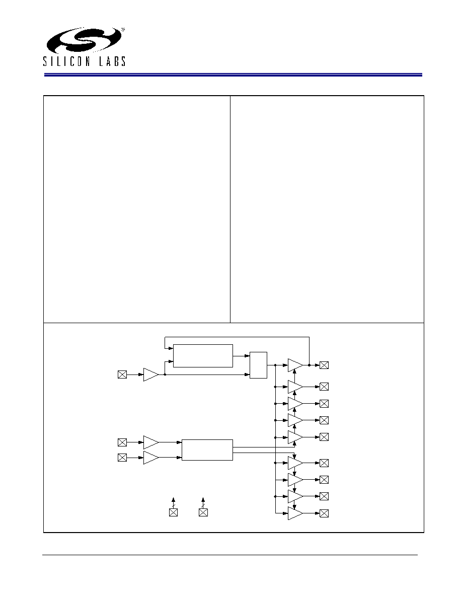
The SL23EP09 is a low skew, low jitter and low power Zero
Delay Buffer (ZDB) designed to produce up to nine (9) clock
outputs from one (1) reference input clock, for high speed
clock distribution applications.
The product has an on-chip PLL which locks to the input
clock at CLKIN and receives its feedback internally from the
CLKOUT pin.
The SL23EP09 has two (2) clock driver banks each with four
(4) clock outputs. These outputs are controlled by two (2)
select input pins S1 and S2. When only four (4) outputs are
needed, four (4) bank-B output clock buffers can be tri-stated
to reduce power dissipation and jitter. The select inputs can
also be used to tri-state both banks A and B or drive them
directly from the input bypassing the PLL and making the
product behave like a Non-Zero Delay Buffer (NZDB).
The high-drive version operates up to 220MHz and 200MHz
at 3.3V and 2.5V power supplies respectively.
Benefits
Up to nine (9) distribution of input clock
Standard and High-Dirive levels to control impedance
level, frequency range and EMI
Low power dissipation, jitter and skew
Low cost
Block Diagram
Low Power and
Low Jitter
PLL
MUX
Input Selection
Decoding Logic
VDD
GND
2
S2
S1
CLKIN
CLKOUT
CLKA1
CLKA2
CLKA3
CLKA4
CLKB1
CLKB2
CLKB3
CLKB4
Low Jitter and Skew 10 to 220 MHz Zero Delay Buffer (ZDB)
相关PDF资料 |
PDF描述 |
|---|---|
| AD5321BRTZ-REEL | IC DAC 12BIT 2WIRE I2C SOT23-6 |
| VI-211-MW-F2 | CONVERTER MOD DC/DC 12V 100W |
| VE-234-MW-F1 | CONVERTER MOD DC/DC 48V 100W |
| V24A5H400BF | CONVERTER MOD DC/DC 5V 400W |
| SL2309ZI-1HT | IC BUFFER 140MHZ 9CH3.3V 16TSSOP |
相关代理商/技术参数 |
参数描述 |
|---|---|
| SL23HE3/2CT | 功能描述:肖特基二极管与整流器 30 Volt 2.0 Amp 100 Amp IFSM RoHS:否 制造商:Skyworks Solutions, Inc. 产品:Schottky Diodes 峰值反向电压:2 V 正向连续电流:50 mA 最大浪涌电流: 配置:Crossover Quad 恢复时间: 正向电压下降:370 mV 最大反向漏泄电流: 最大功率耗散:75 mW 工作温度范围:- 65 C to + 150 C 安装风格:SMD/SMT 封装 / 箱体:SOT-143 封装:Reel |
| SL23HE3/52T | 功能描述:肖特基二极管与整流器 30 Volt 2.0 Amp 100 Amp IFSM RoHS:否 制造商:Skyworks Solutions, Inc. 产品:Schottky Diodes 峰值反向电压:2 V 正向连续电流:50 mA 最大浪涌电流: 配置:Crossover Quad 恢复时间: 正向电压下降:370 mV 最大反向漏泄电流: 最大功率耗散:75 mW 工作温度范围:- 65 C to + 150 C 安装风格:SMD/SMT 封装 / 箱体:SOT-143 封装:Reel |
| SL23HE3/55T | 功能描述:肖特基二极管与整流器 30 Volt 2.0 Amp 100 Amp IFSM RoHS:否 制造商:Skyworks Solutions, Inc. 产品:Schottky Diodes 峰值反向电压:2 V 正向连续电流:50 mA 最大浪涌电流: 配置:Crossover Quad 恢复时间: 正向电压下降:370 mV 最大反向漏泄电流: 最大功率耗散:75 mW 工作温度范围:- 65 C to + 150 C 安装风格:SMD/SMT 封装 / 箱体:SOT-143 封装:Reel |
| SL23HE3/5BT | 功能描述:肖特基二极管与整流器 30 Volt 2.0 Amp 100 Amp IFSM RoHS:否 制造商:Skyworks Solutions, Inc. 产品:Schottky Diodes 峰值反向电压:2 V 正向连续电流:50 mA 最大浪涌电流: 配置:Crossover Quad 恢复时间: 正向电压下降:370 mV 最大反向漏泄电流: 最大功率耗散:75 mW 工作温度范围:- 65 C to + 150 C 安装风格:SMD/SMT 封装 / 箱体:SOT-143 封装:Reel |
| SL23-L | 制造商:FORMOSA 制造商全称:Formosa MS 功能描述:Low VF Chip Schottky Barrier Diodes - Silicon epitaxial planer type |
发布紧急采购,3分钟左右您将得到回复。