- 您现在的位置:买卖IC网 > PDF目录98082 > SL28PCIE26ALC (SILICON LABORATORIES) OTHER CLOCK GENERATOR, QCC32 PDF资料下载
参数资料
| 型号: | SL28PCIE26ALC |
| 厂商: | SILICON LABORATORIES |
| 元件分类: | 时钟产生/分配 |
| 英文描述: | OTHER CLOCK GENERATOR, QCC32 |
| 封装: | 5 X 5 MM, LEAD FREE, QFN-32 |
| 文件页数: | 8/14页 |
| 文件大小: | 232K |
| 代理商: | SL28PCIE26ALC |
SL28PCIe26
DOC#: SP-AP-0774 (Rev. AA)
Page 3 of 14
their default setting at power-up. The use of this interface is
optional. Clock device register changes are normally made at
system initialization, if any are required. The interface cannot
be used during system operation for power management
functions.
Data Protocol
The clock driver serial protocol accepts byte write, byte read,
block write, and block read operations from the controller. For
block write/read operation, access the bytes in sequential
order from lowest to highest (most significant bit first) with the
ability to stop after any complete byte is transferred. For byte
write and byte read operations, the system controller can
access individually indexed bytes. The offset of the indexed
byte is encoded in the command code described in Table 1.
The block write and block read protocol is outlined in Table 2
while Table 3 outlines byte write and byte read protocol. The
slave receiver address is 11010010 (D2h).
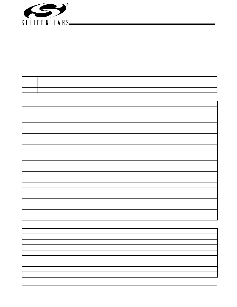
Table 1. Command Code Definition
Bit
Description
7
0 = Block read or block write operation, 1 = Byte read or byte write operation
(6:0)
Byte offset for byte read or byte write operation. For block read or block write operations, these bits should be '0000000'
Table 2. Block Read and Block Write Protocol
Block Write Protocol
Block Read Protocol
Bit
Description
Bit
Description
1Start
1
Start
8:2
Slave address–7 bits
8:2
Slave address–7 bits
9
Write
9
Write
10
Acknowledge from slave
10
Acknowledge from slave
18:11
Command Code–8 bits
18:11
Command Code–8 bits
19
Acknowledge from slave
19
Acknowledge from slave
27:20
Byte Count–8 bits
20
Repeat start
28
Acknowledge from slave
27:21
Slave address–7 bits
36:29
Data byte 1–8 bits
28
Read = 1
37
Acknowledge from slave
29
Acknowledge from slave
45:38
Data byte 2–8 bits
37:30
Byte Count from slave–8 bits
46
Acknowledge from slave
38
Acknowledge
....
Data Byte /Slave Acknowledges
46:39
Data byte 1 from slave–8 bits
....
Data Byte N–8 bits
47
Acknowledge
....
Acknowledge from slave
55:48
Data byte 2 from slave–8 bits
....
Stop
56
Acknowledge
....
Data bytes from slave / Acknowledge
....
Data Byte N from slave–8 bits
....
NOT Acknowledge
....
Stop
Table 3. Byte Read and Byte Write Protocol
Byte Write Protocol
Byte Read Protocol
Bit
Description
Bit
Description
1Start
8:2
Slave address–7 bits
8:2
Slave address–7 bits
9Write
10
Acknowledge from slave
10
Acknowledge from slave
18:11
Command Code–8 bits
18:11
Command Code–8 bits
19
Acknowledge from slave
19
Acknowledge from slave
27:20
Data byte–8 bits
20
Repeated start
相关PDF资料 |
PDF描述 |
|---|---|
| SL28SRC01BZC | OTHER CLOCK GENERATOR, PDSO16 |
| SL38160AZI-18AH | 148.5 MHz, VIDEO CLOCK GENERATOR, PDSO16 |
| SL38160AZC-24AH | 148.5 MHz, VIDEO CLOCK GENERATOR, PDSO16 |
| SL38160ZI-XXXT | 200 MHz, PROC SPECIFIC CLOCK GENERATOR, PDSO16 |
| SL5500_NL | 1 CHANNEL TRANSISTOR OUTPUT OPTOCOUPLER |
相关代理商/技术参数 |
参数描述 |
|---|---|
| SL28PCIe26ALCT | 功能描述:时钟发生器及支持产品 PCIE Clk Gen Xin 25M -->4 PCIE out Gen3 RoHS:否 制造商:Silicon Labs 类型:Clock Generators 最大输入频率:14.318 MHz 最大输出频率:166 MHz 输出端数量:16 占空比 - 最大:55 % 工作电源电压:3.3 V 工作电源电流:1 mA 最大工作温度:+ 85 C 安装风格:SMD/SMT 封装 / 箱体:QFN-56 |
| SL28PCIe26ALI | 功能描述:时钟发生器及支持产品 PCIE Clk Gen Xin 25M -->4 PCIE out Gen3 RoHS:否 制造商:Silicon Labs 类型:Clock Generators 最大输入频率:14.318 MHz 最大输出频率:166 MHz 输出端数量:16 占空比 - 最大:55 % 工作电源电压:3.3 V 工作电源电流:1 mA 最大工作温度:+ 85 C 安装风格:SMD/SMT 封装 / 箱体:QFN-56 |
| SL28PCIe26ALIT | 功能描述:时钟发生器及支持产品 PCIE Clk Gen Xin 25M -->4 PCIE out Gen3 RoHS:否 制造商:Silicon Labs 类型:Clock Generators 最大输入频率:14.318 MHz 最大输出频率:166 MHz 输出端数量:16 占空比 - 最大:55 % 工作电源电压:3.3 V 工作电源电流:1 mA 最大工作温度:+ 85 C 安装风格:SMD/SMT 封装 / 箱体:QFN-56 |
| SL28PCIe30ALC | 功能描述:时钟发生器及支持产品 6outputs 3sngl ended 25MHz crystal input RoHS:否 制造商:Silicon Labs 类型:Clock Generators 最大输入频率:14.318 MHz 最大输出频率:166 MHz 输出端数量:16 占空比 - 最大:55 % 工作电源电压:3.3 V 工作电源电流:1 mA 最大工作温度:+ 85 C 安装风格:SMD/SMT 封装 / 箱体:QFN-56 |
| SL28PCIe30ALCT | 功能描述:时钟发生器及支持产品 6outputs 3sngl ended 25MHz crystal input RoHS:否 制造商:Silicon Labs 类型:Clock Generators 最大输入频率:14.318 MHz 最大输出频率:166 MHz 输出端数量:16 占空比 - 最大:55 % 工作电源电压:3.3 V 工作电源电流:1 mA 最大工作温度:+ 85 C 安装风格:SMD/SMT 封装 / 箱体:QFN-56 |
发布紧急采购,3分钟左右您将得到回复。