- 您现在的位置:买卖IC网 > PDF目录98082 > SM320C25-50FJM (TEXAS INSTRUMENTS INC) 16-BIT, 50 MHz, OTHER DSP, CQCC68 PDF资料下载
参数资料
| 型号: | SM320C25-50FJM |
| 厂商: | TEXAS INSTRUMENTS INC |
| 元件分类: | 数字信号处理 |
| 英文描述: | 16-BIT, 50 MHz, OTHER DSP, CQCC68 |
| 封装: | CERAMIC, MS-004, LCC-68 |
| 文件页数: | 14/40页 |
| 文件大小: | 681K |
| 代理商: | SM320C25-50FJM |
第1页第2页第3页第4页第5页第6页第7页第8页第9页第10页第11页第12页第13页当前第14页第15页第16页第17页第18页第19页第20页第21页第22页第23页第24页第25页第26页第27页第28页第29页第30页第31页第32页第33页第34页第35页第36页第37页第38页第39页第40页
SMJ320C25, SMJ320C2550
DIGITAL SIGNAL PROCESSOR
SGUS007D – AUGUST 1988 – REVISED OCTOBER 2001
21
POST OFFICE BOX 1443
HOUSTON, TEXAS 77251–1443
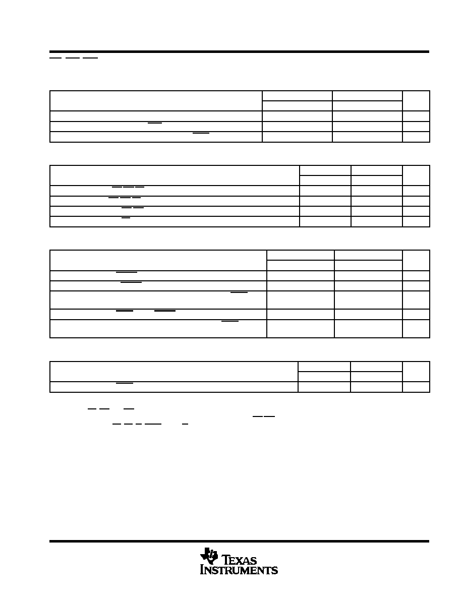
RS, INT, BIO, and XF timing
switching characteristics over recommended operating conditions (see Note 1)
PARAMETER
SMJ320C25-50
SMJ320C25
UNIT
PARAMETER
MIN
TYP
MAX
MIN
TYP
MAX
UNIT
td(RS)
Delay time, CLKOUT1 low to reset state entered
22
ns
td(IACK) Delay time, CLKOUT1 to IACK valid
–5
0
7
–8
0
8
ns
td(XF)
Delay time, XF valid before falling edge of STRB
Q – 10
Q – 12
ns
timing requirements over recommended operating conditions (see Note 1)
SMJ320C25-50
SMJ320C25
UNIT
MIN
MAX
MIN
MAX
UNIT
tsu(IN)
Setup time, INT/BIO/RS before CLKOUT1 high
25
32
ns
th(IN)
Hold time, INT/BIO/RS after CLKOUT1 high
0
ns
tw(IN)
Pulse duration, INT/BIO low
tc(C)
ns
tw(RS)
Pulse duration, RS low
3tc(C)
ns
switching characteristics over recommended operating conditions (see Note 1)
PARAMETER
SMJ320C25-50
SMJ320C25
UNIT
PARAMETER
MIN
TYP
MAX
MIN
TYP
MAX
UNIT
td(C1L-AL) Delay time, HOLDA low after CLKOUT1 low
–1
11
–1
10
ns
tdis(AL-A) Disable time, HOLDA low to address three-state
0
ns
tdis(C1L-A)
Disable time, address three-state after CLKOUT1 low (HOLD
mode, see Note 7 )
20
ns
td(HH-AH) Delay time, HOLD high to HOLDA high
19
25
ns
ten(A-C1L)
Enable time, address driven before CLKOUT1 low (HOLD mode,
see Note 7 )
8
ns
timing requirements over recommended operating conditions (see Note 1)
SMJ320C25-50
SMJ320C25
UNIT
MIN
MAX
MIN
MAX
UNIT
td(C2H-H) Delay time, HOLD valid after CLKOUT2 high
Q – 19
Q – 24
ns
These values are derived from characterization data and not tested.
NOTES:
1. Q = 1/4tc(C)
6. RS, INT, and BIO are asynchronous inputs and can occur at any time during a clock cycle. However, if the specified setup time is
met, the exact sequence shown in the timing diagram occurs. INT/BIO fall time must be less than 8 ns.
7. A15–A0, PS, DS, IS, STRB, and R/W timings are all included in timings referenced as ’”address”.
相关PDF资料 |
PDF描述 |
|---|---|
| SM320C2550GBM | 16-BIT, 50 MHz, OTHER DSP, CPGA68 |
| SM320C30HFGM50 | 32-BIT, 50 MHz, OTHER DSP, CQFP196 |
| SM320C31GFM27 | 32-BIT, 27 MHz, OTHER DSP, CPGA141 |
| SM320C30HUM25 | 32-BIT, 25 MHz, OTHER DSP, CQFP196 |
| SM320C30HTM28 | 32-BIT, 28 MHz, OTHER DSP, CQFP196 |
相关代理商/技术参数 |
参数描述 |
|---|---|
| SM320C25FJM | 制造商:未知厂家 制造商全称:未知厂家 功能描述:16-Bit Digital Signal Processor |
| SM320C25GBM | 制造商:未知厂家 制造商全称:未知厂家 功能描述:16-Bit Digital Signal Processor |
| SM320C26BFJM | 制造商:Texas Instruments 功能描述:DSP FIX PT 16BIT 40MHZ 10MIPS 68PIN JLCC - Rail/Tube |
| SM320C26BGBM | 制造商:TI 制造商全称:Texas Instruments 功能描述:DIGITAL SIGNAL PROCESSOR |
| SM320C2810-EP | 制造商:TI 制造商全称:Texas Instruments 功能描述:Digital Signal Processors |
发布紧急采购,3分钟左右您将得到回复。