- 您现在的位置:买卖IC网 > PDF目录98083 > SM5L3 (SHARP ELECTRONICS CORP) 4-BIT, MROM, MICROCONTROLLER, PQFP80 PDF资料下载
参数资料
| 型号: | SM5L3 |
| 厂商: | SHARP ELECTRONICS CORP |
| 元件分类: | 微控制器/微处理器 |
| 英文描述: | 4-BIT, MROM, MICROCONTROLLER, PQFP80 |
| 封装: | 14 X 20 MM, PLASTIC, QFP-80 |
| 文件页数: | 16/27页 |
| 文件大小: | 164K |
| 代理商: | SM5L3 |
第1页第2页第3页第4页第5页第6页第7页第8页第9页第10页第11页第12页第13页第14页第15页当前第16页第17页第18页第19页第20页第21页第22页第23页第24页第25页第26页第27页
4-Bit Single Chip Microcomputers
SM5L1/SM5L2/SM5L3
Microcomputer Data Sheet
23
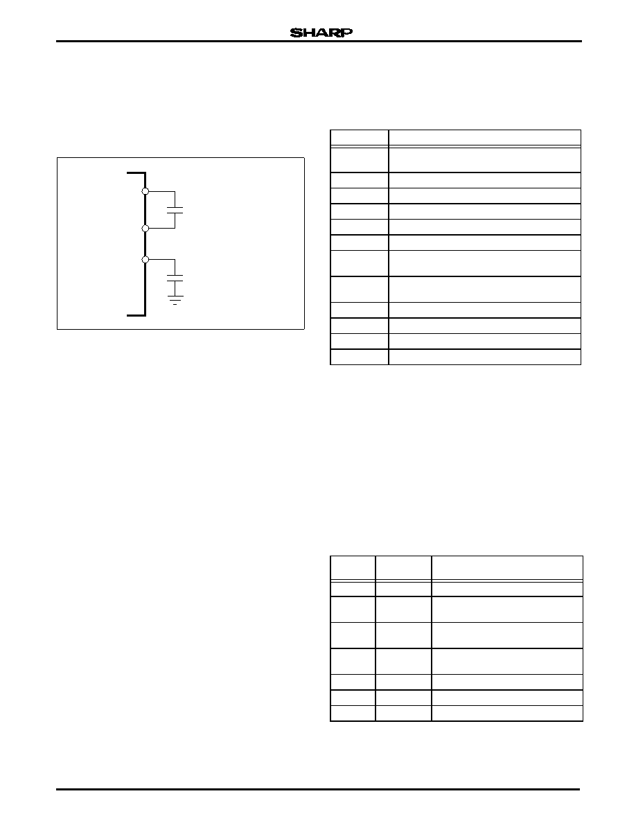
BOOSTER CIRCUIT
The device contains a booster circuit which gener-
ates a voltage two time higher than 1.5 V power supply.
It is necessary to apply external capacitors between
DDC pin and VCC pin as well as VDD pin and GND (see
Figure 30).
BLANK DISPLAY
There are two ways blank the entire display to match
the purpose.
Blanking the display for a short time
– Set bit 0 of the RF register to ‘1’: Display
– Set bit 0 of the RF register to ‘0’: Blank state
Blanking the display for a long period mainly to
reduce supply current.
– Set bit 0 and 1 of the RF register to ‘1’: Display
– Set bit 0 and 1 of the RF register to ‘0’: Blank state
When bit 1 of the RF register is set ‘0’, the booster cir-
cuit does not operate and the common outputs and seg-
ment outputs are fixed to VM level, and the display
blanks. By cutting off the function of the booster circuit,
the supply current can be greatly reduced. However,
when the display is blanked using the second method,
the response speed of the LCD returning to the display
state drops slightly. The RF register is on the blank state
after initialization (reset state) from hardware reset.
INSTRUCTION SET
Definition of Symbols
The following symbols are used in descriptions for
the instructions.
Each bit of a register can be represented. For exam-
ple the ith bit of X register and R(0) register are rep-
resented as Xi and R(0) i. (i = 0, 1, 2, 3, …)
Increment and decrement denote the binary addition
of 1H and FH, respectively.
To skip a certain instruction means that the instruc-
tion is ignored and that no operation is performed
until the execution transfers to the next instruction. In
other words, the instruction is regarded as a NOP
instruction. Therefore, one cycle is required to skip a
one-word instruction and two cycles are required to
skip a two word instruction.
ROM Address Control Instructions
Figure 30. Booster Circuit
C1 = 0.1 F (TYP.)
C2 = 0.1 F (TYP.)
5L1-30
SM5Lx
DDC
VCC
VDD
SYMBOL
DEFINITION
M
Content of RAM at the address specified by
the B register
←
Transfer direction
∪
Logical OR
∩
Logical AND
⊕
Logical XOR
Ai
ith bit of the ACC
Push
Contents of the PC are decremented to the
stack register
Pop
The decremented contents are transferred
back to the PC
Pj
Pj register (j = 3, 2, 1, 0)
Rj
Rj register (j = F, E, D)
ROM (
)
ROM contents for address within (
)
Cy
Carry of ALU (different from the C flag)
MNE-
MONIC
MACHINE
CODE
OPERATIONS
TR x
80 to BF
PL ← x (I5 –I0)
TL xy
E0 to EF
00 to FF
PU ← x (I11 –I6)
PL ← y (I5 –I0)
TRS x
C0 to DF
Push, PU ← 01H,
PL ← x (I4, I3, I2, I1, I0, 0)
CALL xy
F0 to FF
00 to FF
Push, PU ← x (I11 –I6)
PL ← y (I5 – I0)
RTN
7D
Pop
RTNS
7E
Pop, skip the next step
RTNI
7F
Pop, IME
← 1
相关PDF资料 |
PDF描述 |
|---|---|
| SM802104UMG | 212.5 MHz, OTHER CLOCK GENERATOR, QCC24 |
| SM802105UMG | 312.5 MHz, OTHER CLOCK GENERATOR, QCC24 |
| SM802108UMG | 156.25 MHz, OTHER CLOCK GENERATOR, QCC24 |
| SMC34C90 | PCI BUS CONTROLLER, PBGA256 |
| SMC6247 | 4-BIT, MROM, 1 MHz, MICROCONTROLLER, PQFP160 |
相关代理商/技术参数 |
参数描述 |
|---|---|
| SM5LS | 制造商:Potter & Brumfield 功能描述:RELAY SPDT .25A 5000 ohm special |
| SM5LS-5000 | 制造商:P&B 功能描述: 制造商:TE Connectivity 功能描述: |
| SM5M2 | 制造商:SHARP 制造商全称:Sharp Electrionic Components 功能描述:4-Bit Single-Chip Microcomputer(LCD Driver) |
| SM-5R1000FE6 | 功能描述:RES 0.1 OHM 1% 4W 制造商:vishay dale 系列:SM 包装:剪切带(CT) 零件状态:Digi-Key 停止供應 电阻值:100 mOhms 容差:±1% 功率(W):4W 成分:绕线 特性:- 温度系数:- 工作温度:-55°C ~ 275°C 封装/外壳:8230 J 形引线 供应商器件封装:SM-5 大小/尺寸:0.820" 长 x 0.295" 宽(20.83mm x 7.49mm) 高度 - 安装(最大值):0.305"(7.75mm) 端子数:2 故障率:- 标准包装:1 |
| SM-5R5000FE6 | 功能描述:RES 0.5 OHM 1% 4W 制造商:vishay dale 系列:SM 包装:剪切带(CT) 零件状态:Digi-Key 停止供應 电阻值:500 mOhms 容差:±1% 功率(W):4W 成分:绕线 特性:- 温度系数:- 工作温度:-55°C ~ 275°C 封装/外壳:8230 J 形引线 供应商器件封装:SM-5 大小/尺寸:0.820" 长 x 0.295" 宽(20.83mm x 7.49mm) 高度 - 安装(最大值):0.305"(7.75mm) 端子数:2 故障率:- 标准包装:1 |
发布紧急采购,3分钟左右您将得到回复。