- 您现在的位置:买卖IC网 > PDF目录98106 > SN74AUP1G17DBVRG4 (TEXAS INSTRUMENTS INC) AUP/ULP/V SERIES, 1-INPUT NON-INVERT GATE, PDSO5 PDF资料下载
参数资料
| 型号: | SN74AUP1G17DBVRG4 |
| 厂商: | TEXAS INSTRUMENTS INC |
| 元件分类: | 门电路 |
| 英文描述: | AUP/ULP/V SERIES, 1-INPUT NON-INVERT GATE, PDSO5 |
| 封装: | GREEN, PLASTIC, SOT-23, 5 PIN |
| 文件页数: | 20/25页 |
| 文件大小: | 1080K |
| 代理商: | SN74AUP1G17DBVRG4 |
SCES579I – JUNE 2004 – REVISED MARCH 2010
www.ti.com
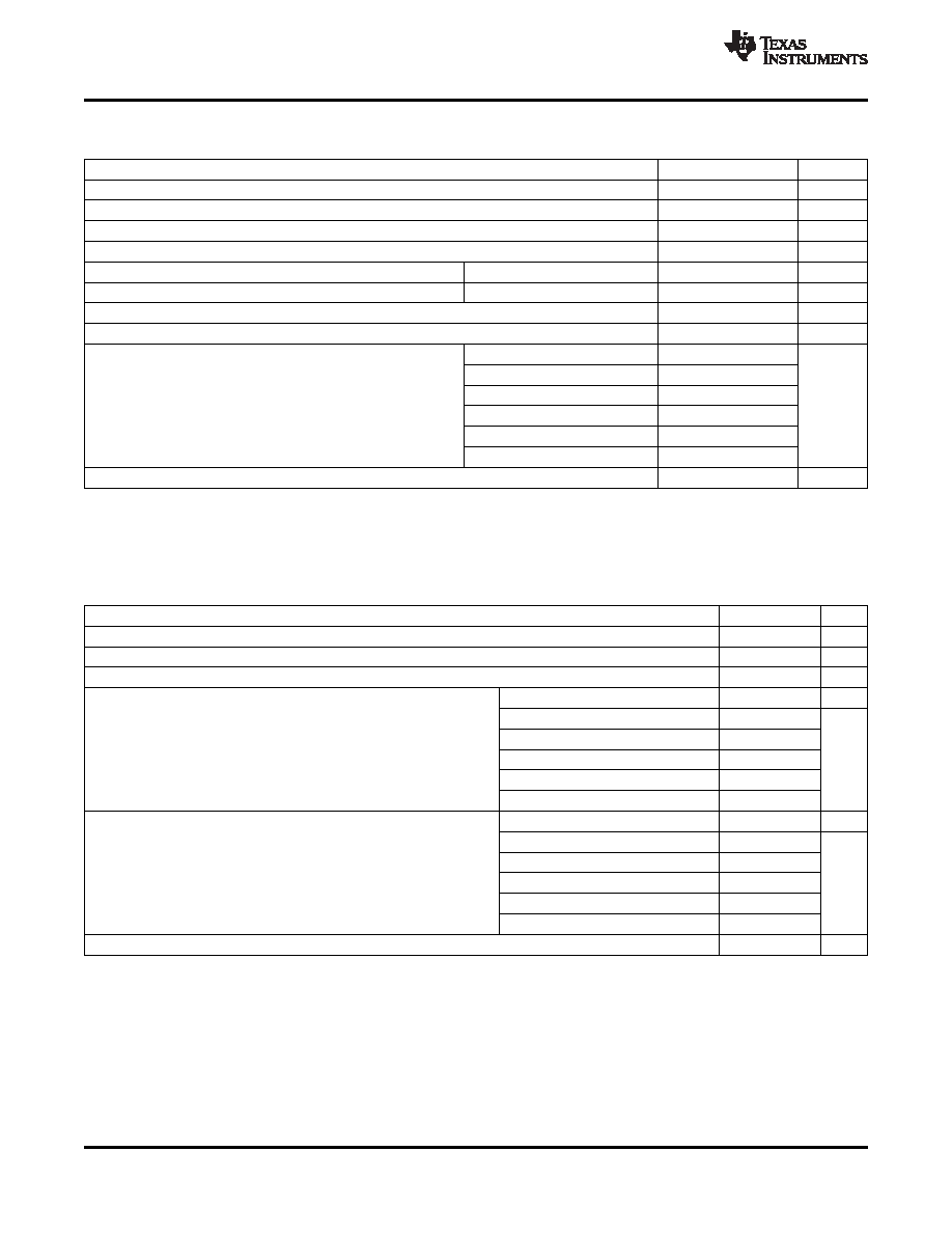
ABSOLUTE MAXIMUM RATINGS
(1)
over operating free-air temperature range (unless otherwise noted)
MIN
MAX
UNIT
VCC
Supply voltage range
–0.5
4.6
V
VI
Input voltage range(2)
–0.5
4.6
V
VO
Voltage range applied to any output in the high-impedance or power-off state(2)
–0.5
4.6
V
VO
Output voltage range in the high or low state(2)
–0.5
VCC + 0.5
V
IIK
Input clamp current
VI < 0
–50
mA
IOK
Output clamp current
VO < 0
–50
mA
IO
Continuous output current
±20
mA
Continuous current through VCC or GND
±50
mA
DBV package
206
DCK package
252
DRL package
142
qJA
Package thermal impedance(3)
°C/W
DSF package
300
DRY package
234
YFP/YZP package
132
Tstg
Storage temperature range
–65
150
°C
(1)
Stresses beyond those listed under "absolute maximum ratings" may cause permanent damage to the device. These are stress ratings
only, and functional operation of the device at these or any other conditions beyond those indicated under "recommended operating
conditions" is not implied. Exposure to absolute-maximum-rated conditions for extended periods may affect device reliability.
(2)
The input and output negative-voltage ratings may be exceeded if the input and output current ratings are observed.
(3)
The package thermal impedance is calculated in accordance with JESD 51-7.
RECOMMENDED OPERATING CONDITIONS
(1)
MIN
MAX
UNIT
VCC
Supply voltage
0.8
3.6
V
VI
Input voltage
0
3.6
V
VO
Output voltage
0
VCC
V
VCC = 0.8 V
–20
mA
VCC = 1.1 V
–1.1
VCC = 1.4 V
–1.7
IOH
(2)
High-level output current
VCC = 1.65
–1.9
mA
VCC = 2.3 V
–3.1
VCC = 3 V
–4
VCC = 0.8 V
20
mA
VCC = 1.1 V
1.1
VCC = 1.4 V
1.7
IOL
(2)
Low-level output current
VCC = 1.65 V
1.9
mA
VCC = 2.3 V
3.1
VCC = 3 V
4
TA
Operating free-air temperature
–40
85
°C
(1)
All unused inputs of the device must be held at VCC or GND to ensure proper device operation. Refer to the TI application report,
Implications of Slow or Floating CMOS Inputs, literature number SCBA004.
(2)
Defined by the signal-integrity requirements and design-goal priorities
4
Copyright 2004–2010, Texas Instruments Incorporated
Product Folder Link(s): SN74AUP1G17
相关PDF资料 |
PDF描述 |
|---|---|
| SN74AUP1G17MDCKREP | AUP/ULP/V SERIES, 1-INPUT NON-INVERT GATE, PDSO5 |
| SN74AUP1G240DBVT | AUP/ULP/V SERIES, 1-BIT DRIVER, INVERTED OUTPUT, PDSO5 |
| SN74AUP1G240YEPR | AUP/ULP/V SERIES, 1-BIT DRIVER, INVERTED OUTPUT, BGA5 |
| SN74AUP1G32DCKT | AUP/ULP/V SERIES, 2-INPUT OR GATE, PDSO5 |
| SN74AUP1G34DCKT | AUP/ULP/V SERIES, 1-INPUT NON-INVERT GATE, PDSO5 |
相关代理商/技术参数 |
参数描述 |
|---|---|
| SN74AUP1G17DBVT | 功能描述:缓冲器和线路驱动器 Lo PWR SNGL Schmitt Trgr Bufr RoHS:否 制造商:Micrel 输入线路数量:1 输出线路数量:2 极性:Non-Inverting 电源电压-最大:+/- 5.5 V 电源电压-最小:+/- 2.37 V 最大工作温度:+ 85 C 安装风格:SMD/SMT 封装 / 箱体:MSOP-8 封装:Reel |
| SN74AUP1G17DBVTE4 | 功能描述:缓冲器和线路驱动器 Lo PWR SNGL Schmitt Trgr Bufr RoHS:否 制造商:Micrel 输入线路数量:1 输出线路数量:2 极性:Non-Inverting 电源电压-最大:+/- 5.5 V 电源电压-最小:+/- 2.37 V 最大工作温度:+ 85 C 安装风格:SMD/SMT 封装 / 箱体:MSOP-8 封装:Reel |
| SN74AUP1G17DBVTG4 | 功能描述:缓冲器和线路驱动器 Lo PWR SNGL Schmitt Trgr Bufr RoHS:否 制造商:Micrel 输入线路数量:1 输出线路数量:2 极性:Non-Inverting 电源电压-最大:+/- 5.5 V 电源电压-最小:+/- 2.37 V 最大工作温度:+ 85 C 安装风格:SMD/SMT 封装 / 箱体:MSOP-8 封装:Reel |
| SN74AUP1G17DCKR | 功能描述:缓冲器和线路驱动器 Lo-Pwr Sgle Schmitt- Trigger Inverter RoHS:否 制造商:Micrel 输入线路数量:1 输出线路数量:2 极性:Non-Inverting 电源电压-最大:+/- 5.5 V 电源电压-最小:+/- 2.37 V 最大工作温度:+ 85 C 安装风格:SMD/SMT 封装 / 箱体:MSOP-8 封装:Reel |
| SN74AUP1G17DCKRE4 | 功能描述:缓冲器和线路驱动器 Lo PWR SNGL Schmitt Trgr Bufr RoHS:否 制造商:Micrel 输入线路数量:1 输出线路数量:2 极性:Non-Inverting 电源电压-最大:+/- 5.5 V 电源电压-最小:+/- 2.37 V 最大工作温度:+ 85 C 安装风格:SMD/SMT 封装 / 箱体:MSOP-8 封装:Reel |
发布紧急采购,3分钟左右您将得到回复。