- 您现在的位置:买卖IC网 > PDF目录98111 > SN74CBTLV3384DW (TEXAS INSTRUMENTS INC) CBTLV/3B SERIES, DUAL 5-BIT DRIVER, TRUE OUTPUT, PDSO24 PDF资料下载
参数资料
| 型号: | SN74CBTLV3384DW |
| 厂商: | TEXAS INSTRUMENTS INC |
| 元件分类: | 总线收发器 |
| 英文描述: | CBTLV/3B SERIES, DUAL 5-BIT DRIVER, TRUE OUTPUT, PDSO24 |
| 封装: | GREEN, PLASTIC, SOIC-24 |
| 文件页数: | 8/14页 |
| 文件大小: | 494K |
| 代理商: | SN74CBTLV3384DW |
SN74CBTLV3384
LOW-VOLTAGE 10-BIT FET BUS SWITCH
SCDS059G MARCH 1998 REVISED JUNE 2004
3
POST OFFICE BOX 655303
DALLAS, TEXAS 75265
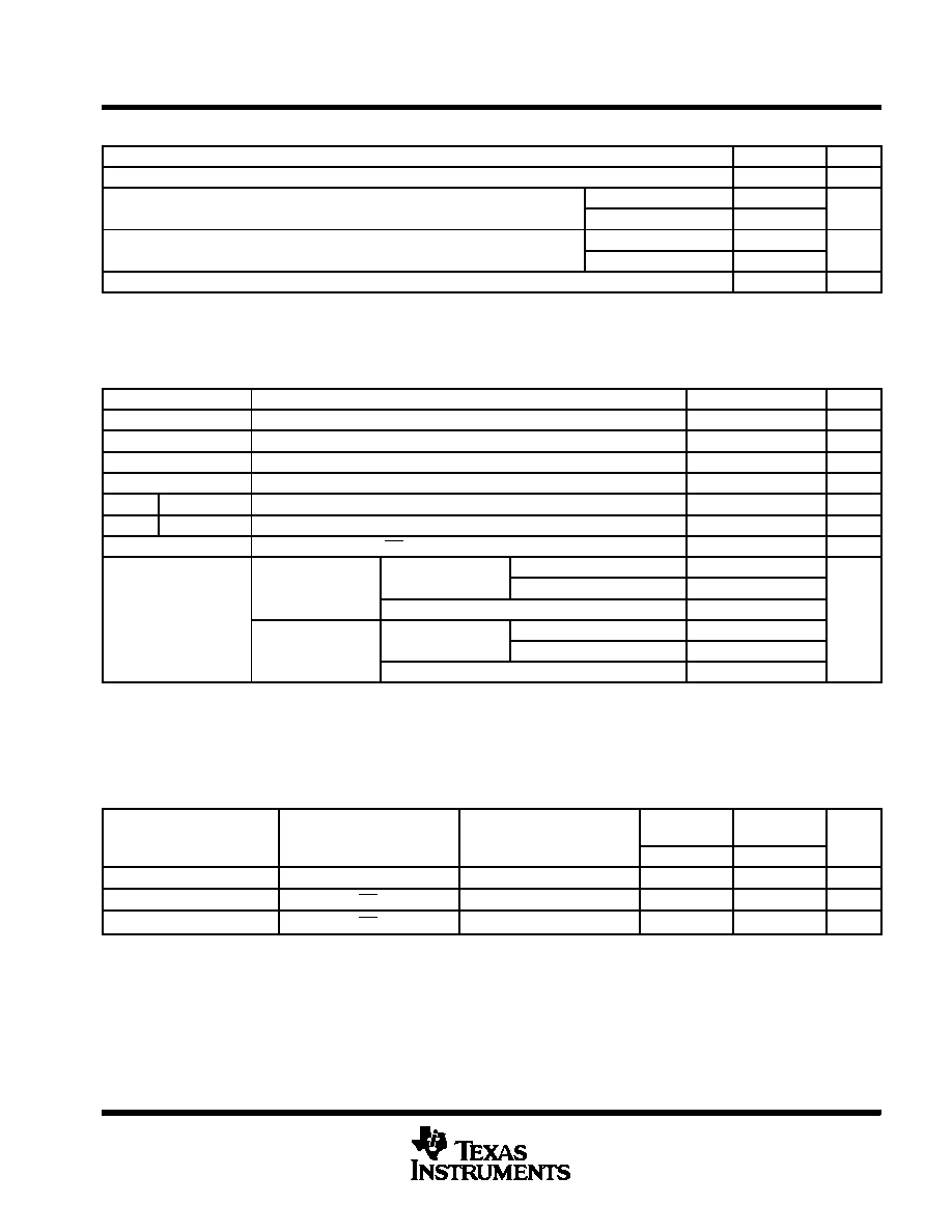
recommended operating conditions (see Note 3)
MIN
MAX
UNIT
VCC
Supply voltage
2.3
3.6
V
High level control input voltage
VCC = 2.3 V to 2.7 V
1.7
V
VIH
High-level control input voltage
VCC = 2.7 V to 3.6 V
2
V
Low level control input voltage
VCC = 2.3 V to 2.7 V
0.7
V
VIL
Low-level control input voltage
VCC = 2.7 V to 3.6 V
0.8
V
TA
Operating free-air temperature
40
85
°C
NOTE 3: All unused control inputs of the device must be held at VCC or GND to ensure proper device operation. Refer to the TI application report,
Implications of Slow or Floating CMOS Inputs, literature number SCBA004.
electrical characteristics over recommended operating free-air temperature range (unless
otherwise noted)
PARAMETER
TEST CONDITIONS
MIN
TYP
MAX
UNIT
VIK
VCC = 3 V,
II = 18 mA
1.2
V
II
VCC = 3.6 V,
VI = VCC or GND
±1
μA
Ioff
VCC = 0,
VI or VO = 0 to 3.6 V
10
μA
ICC
VCC = 3.6 V,
IO = 0,
VI = VCC or GND
10
μA
ΔICC
Control inputs
VCC = 3.6 V,
One input at 3 V,
Other inputs at VCC or GND
300
μA
Ci
Control inputs
VI = 3 V or 0
4.5
pF
Cio(OFF)
VO = 3 V or 0,
OE = VCC
10
pF
V
23V
V
0
II = 64 mA
5
8
VCC = 2.3 V,
TYP at VCC =25V
VI = 0
II = 24 mA
5
8
r §
TYP at VCC = 2.5 V
VI = 1.7 V,
II = 15 mA
27
40
Ω
ron§
V
0
II = 64 mA
5
7
Ω
VCC = 3 V
VI = 0
II = 24 mA
5
7
CC
VI = 2.4 V,
II = 15 mA
10
15
All typical values are at VCC = 3.3 V (unless otherwise noted), TA = 25°C.
This is the increase in supply current for each input that is at the specified voltage level, rather than VCC or GND.
§ Measured by the voltage drop between the A and B terminals at the indicated current through the switch. On-state resistance is determined by
the lower of the voltages of the two (A or B) terminals.
switching characteristics over recommended operating free-air temperature range (unless
otherwise noted) (see Figure 1)
PARAMETER
FROM
(INPUT)
TO
(OUTPUT)
VCC = 2.5 V
± 0.2 V
VCC = 3.3 V
± 0.3 V
UNIT
PARAMETER
(INPUT)
(OUTPUT)
MIN
MAX
MIN
MAX
UNIT
tpd
A or B
B or A
0.15
0.25
ns
ten
OE
A or B
1
5
1
4.3
ns
tdis
OE
A or B
1
5.5
1
5.5
ns
The propagation delay is the calculated RC time constant of the typical on-state resistance of the switch and the specified load capacitance, when
driven by an ideal voltage source (zero output impedance).
相关PDF资料 |
PDF描述 |
|---|---|
| SN74CBTLV3857DBQR | CBTLV/3B SERIES, 10-BIT DRIVER, TRUE OUTPUT, PDSO24 |
| SN74CBTLV3861PWR | CBTLV/3B SERIES, 10-BIT DRIVER, TRUE OUTPUT, PDSO24 |
| SN74CBTLV3861DWG4 | CBTLV/3B SERIES, 10-BIT DRIVER, TRUE OUTPUT, PDSO24 |
| SN74CBTS3306PWRG4 | CBT/FST/QS/5C/B SERIES, 2-BIT DRIVER, TRUE OUTPUT, PDSO8 |
| SN74CBTS3384DWE4 | CBT/FST/QS/5C/B SERIES, 10-BIT DRIVER, TRUE OUTPUT, PDSO24 |
相关代理商/技术参数 |
参数描述 |
|---|---|
| SN74CBTLV3384DWE4 | 功能描述:数字总线开关 IC 16-Bit Edg-Trig D-Ty F-F W/3-State Otpt RoHS:否 制造商:Texas Instruments 开关数量:24 传播延迟时间:0.25 ns 最大工作温度:+ 85 C 最小工作温度:- 40 C 封装 / 箱体:TSSOP-56 封装:Reel |
| SN74CBTLV3384DWG4 | 功能描述:数字总线开关 IC LO VLTG 10B FETBus Switch RoHS:否 制造商:Texas Instruments 开关数量:24 传播延迟时间:0.25 ns 最大工作温度:+ 85 C 最小工作温度:- 40 C 封装 / 箱体:TSSOP-56 封装:Reel |
| SN74CBTLV3384DWR | 功能描述:数字总线开关 IC LV 10-Bit FET RoHS:否 制造商:Texas Instruments 开关数量:24 传播延迟时间:0.25 ns 最大工作温度:+ 85 C 最小工作温度:- 40 C 封装 / 箱体:TSSOP-56 封装:Reel |
| SN74CBTLV3384PW | 功能描述:数字总线开关 IC Low-Voltage 10-Bit FET Bus Switch RoHS:否 制造商:Texas Instruments 开关数量:24 传播延迟时间:0.25 ns 最大工作温度:+ 85 C 最小工作温度:- 40 C 封装 / 箱体:TSSOP-56 封装:Reel |
| SN74CBTLV3384PWE4 | 功能描述:数字总线开关 IC 16-Bit Edg-Trig D-Ty F-F W/3-State Otpt RoHS:否 制造商:Texas Instruments 开关数量:24 传播延迟时间:0.25 ns 最大工作温度:+ 85 C 最小工作温度:- 40 C 封装 / 箱体:TSSOP-56 封装:Reel |
发布紧急采购,3分钟左右您将得到回复。