- 您现在的位置:买卖IC网 > PDF目录98116 > SN74LS06DRG4 (TEXAS INSTRUMENTS INC) LS SERIES, HEX 1-INPUT INVERT GATE, PDSO14 PDF资料下载
参数资料
| 型号: | SN74LS06DRG4 |
| 厂商: | TEXAS INSTRUMENTS INC |
| 元件分类: | 门电路 |
| 英文描述: | LS SERIES, HEX 1-INPUT INVERT GATE, PDSO14 |
| 封装: | GREEN, PLASTIC, SOIC-14 |
| 文件页数: | 11/17页 |
| 文件大小: | 641K |
| 代理商: | SN74LS06DRG4 |
SN54LS06, SN74LS06, SN74LS16
HEX INVERTER BUFFERS/DRIVERS
WITH OPENCOLLECTOR HIGHVOLTAGE OUTPUTS
SDLS020E MAY 1990 REVISED FEBRUARY 2004
3
POST OFFICE BOX 655303
DALLAS, TEXAS 75265
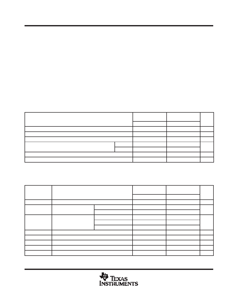
absolute maximum ratings over operating free-air temperature range (unless otherwise noted)
Supply voltage, VCC
7 V
. . . . . . . . . . . . . . . . . . . . . . . . . . . . . . . . . . . . . . . . . . . . . . . . . . . . . . . . . . . . . . . . . . . . . . . .
Input voltage, VI (see Note 1)
7 V
. . . . . . . . . . . . . . . . . . . . . . . . . . . . . . . . . . . . . . . . . . . . . . . . . . . . . . . . . . . . . . . . .
Output voltage, VO (see Notes 1 and 2): SN54LS06, SN74LS06
30 V
. . . . . . . . . . . . . . . . . . . . . . . . . . . . . . . . .
SN74LS16
15 V
. . . . . . . . . . . . . . . . . . . . . . . . . . . . . . . . . . . . . . . . . . . .
Package thermal impedance,
θJA (see Note 3): D package
86
°C/W
. . . . . . . . . . . . . . . . . . . . . . . . . . . . . . . . . . .
DB package
96
°C/W
. . . . . . . . . . . . . . . . . . . . . . . . . . . . . . . . .
N package
80
°C/W
. . . . . . . . . . . . . . . . . . . . . . . . . . . . . . . . . . .
NS package
76
°C/W
. . . . . . . . . . . . . . . . . . . . . . . . . . . . . . . . .
Storage temperature range, Tstg
65
°C to 150°C
. . . . . . . . . . . . . . . . . . . . . . . . . . . . . . . . . . . . . . . . . . . . . . . . . . .
Stresses beyond those listed under “absolute maximum ratings” may cause permanent damage to the device. These are stress ratings only, and
functional operation of the device at these or any other conditions beyond those indicated under “recommended operating conditions” is not
implied. Exposure to absolute-maximum-rated conditions for extended periods may affect device reliability.
NOTES:
1. All voltage values are with respect to GND.
2. This is the maximum voltage that should be applied to any output when it is in the off state.
3. The package thermal impedance is calculated in accordance with JESD 51-7.
recommended operating conditions (see Note 4)
SN54LS06
SN74LS06
SN74LS16
UNIT
MIN
NOM
MAX
MIN
NOM
MAX
UNIT
VCC
Supply voltage
4.5
5
5.5
4.75
5
5.25
V
VIH
High-level input voltage
2
V
VIL
Low-level input voltage
0.8
V
VOH
High-level output voltage
’LS06
30
V
VOH
High-level output voltage
SN74LS16
15
V
IOL
Low-level output current
30
40
mA
TA
Operating free-air temperature
55
125
0
70
°C
NOTE 4: All unused inputs of the device must be held at VCC or GND to ensure proper device operation. Refer to the TI application report,
Implications of Slow or Floating CMOS Inputs, literature number SCBA004.
electrical characteristics over recommended operating free-air temperature range (unless
otherwise noted)
PARAMETER
TEST CONDITIONS
SN54LS06
SN74LS06
SN74LS16
UNIT
PARAMETER
TEST CONDITIONS
MIN
TYP§
MAX
MIN
TYP§
MAX
UNIT
VIK
VCC = MIN,
II = 12 mA
1.5
V
IOH
VCC = MIN,
VIL = 0.8 V
’LS06,
VOH = 30 V
0.25
mA
IOH
VCC = MIN,
VIL = 0.8 V
SN74LS16,
VOH = 15 V
0.25
mA
IOL = 16 mA
0.25
0.4
0.25
0.4
VOL
VCC = MIN,
VIH = 2 V
IOL = 30 mA
0.7
V
VOL
VCC = MIN,
VIH = 2 V
IOL = 40 mA
0.7
V
II
VCC = MAX,
VI = 7 V
1
mA
IIH
VCC = MAX,
VI = 2.4 V
20
A
IIL
VCC = MAX,
VI = 0.4 V
0.2
mA
ICCH
VCC = MAX
18
mA
ICCL
VCC = MAX
60
mA
For conditions shown as MIN or MAX, use the appropriate value specified under recommended operating conditions.
§ All typical values are at VCC = 5 V, and TA = 25°C.
The SN74LS16 is obsolete
and is no longer supplied.
相关PDF资料 |
PDF描述 |
|---|---|
| SN74LS173ANSRG4 | LS SERIES, POSITIVE EDGE TRIGGERED D FLIP-FLOP, TRUE OUTPUT, PDSO16 |
| SN74LS173ANSR | LS SERIES, POSITIVE EDGE TRIGGERED D FLIP-FLOP, TRUE OUTPUT, PDSO16 |
| SN74LS175NS | LS SERIES, POSITIVE EDGE TRIGGERED D FLIP-FLOP, COMPLEMENTARY OUTPUT, PDSO16 |
| SN74LS17DR | LS SERIES, HEX 1-INPUT NON-INVERT GATE, PDSO14 |
| SN74LS07DR | LS SERIES, HEX 1-INPUT NON-INVERT GATE, PDSO14 |
相关代理商/技术参数 |
参数描述 |
|---|---|
| SN74LS06N | 功能描述:缓冲器和线路驱动器 Hex inverter Buffer/ Driver RoHS:否 制造商:Micrel 输入线路数量:1 输出线路数量:2 极性:Non-Inverting 电源电压-最大:+/- 5.5 V 电源电压-最小:+/- 2.37 V 最大工作温度:+ 85 C 安装风格:SMD/SMT 封装 / 箱体:MSOP-8 封装:Reel |
| SN74LS06N | 制造商:Texas Instruments 功能描述:IC BUFFER/DRIVER/RECEIVER |
| SN74LS06N | 制造商:Texas Instruments 功能描述:Buffer / Driver / Receiver Logic IC |
| SN74LS06NE4 | 功能描述:缓冲器和线路驱动器 Hex inverter Buffer/ Driver RoHS:否 制造商:Micrel 输入线路数量:1 输出线路数量:2 极性:Non-Inverting 电源电压-最大:+/- 5.5 V 电源电压-最小:+/- 2.37 V 最大工作温度:+ 85 C 安装风格:SMD/SMT 封装 / 箱体:MSOP-8 封装:Reel |
| SN74LS06NG4 | 制造商:Texas Instruments 功能描述:HEX INVERTER BUFFER/DRIVER 74LC06 制造商:Texas Instruments 功能描述:HEX INVERTER BUFFER/DRIVER, 74LC06 制造商:Texas Instruments 功能描述:HEX INVERTER BUFFER/DRIVER, 74LC06; Logic Device Type:Buffer / Driver, Inverting; Supply Voltage Min:4.75V; Supply Voltage Max:5.25V; Logic Case Style:DIP; No. of Pins:14; Operating Temperature Min:0C; Operating Temperature ;RoHS Compliant: Yes |
发布紧急采购,3分钟左右您将得到回复。