- 您现在的位置:买卖IC网 > PDF目录97085 > SN74LV573DWR (TEXAS INSTRUMENTS INC) LV/LV-A/LVX/H SERIES, 8-BIT DRIVER, TRUE OUTPUT, PDSO20 PDF资料下载
参数资料
| 型号: | SN74LV573DWR |
| 厂商: | TEXAS INSTRUMENTS INC |
| 元件分类: | 总线收发器 |
| 英文描述: | LV/LV-A/LVX/H SERIES, 8-BIT DRIVER, TRUE OUTPUT, PDSO20 |
| 封装: | PLASTIC, SO-20 |
| 文件页数: | 1/8页 |
| 文件大小: | 145K |
| 代理商: | SN74LV573DWR |
SN54LV573, SN74LV573
OCTAL TRANSPARENT DTYPE LATCHES
WITH 3STATE OUTPUTS
SCLS198B FEBRUARY 1993 REVISED APRIL 1996
1
POST OFFICE BOX 655303
DALLAS, TEXAS 75265
POST OFFICE BOX 1443
HOUSTON, TEXAS 772511443
D EPIC (Enhanced-Performance Implanted
CMOS) 2-
Process
D Typical VOLP (Output Ground Bounce)
< 0.8 V at VCC, TA = 25°C
D Typical VOHV (Output VOH Undershoot)
> 2 V at VCC, TA = 25°C
D ESD Protection Exceeds 2000 V Per
MIL-STD-883C, Method 3015; Exceeds
200 V Using Machine Model
(C = 200 pF, R = 0)
D Latch-Up Performance Exceeds 250 mA
Per JEDEC Standard JESD-17
D Package Options Include Plastic
Small-Outline (DW), Shrink Small-Outline
(DB), Thin Shrink Small-Outline (PW),
Ceramic Flat (W) Packages, Chip Carriers
(FK), and (J) 300-mil DIPs
description
These octal transparent D-type latches are
designed for 2.7-V to 5.5-V VCC operation.
The ’LV573 feature 3-state outputs designed
specifically for driving highly capacitive or
relatively low-impedance loads. This device is
particularly suitable for implementing buffer
registers, I/O ports, bidirectional bus drivers, and
working registers.
While the latch-enable (LE) input is high, the Q outputs follow the data (D) inputs. When LE is taken low, the
Q outputs are latched at the logic levels set up at the D inputs.
A buffered output-enable (OE) input can be used to place the eight outputs in either a normal logic state (high
or low logic levels) or high-impedance state. In the high-impedance state, the outputs neither load nor drive the
bus lines significantly. The high-impedance state and increased drive provide the capability to drive bus lines
without need for interface or pullup components.
OE does not affect the internal operations of the latches. Old data can be retained or new data can be entered
while the outputs are in the high-impedance state.
The SN74LV573 is available in TI’s shrink small-outline package (DB), which provides the same I/O pin count
and functionality of standard small-outline packages in less than half the printed-circuit-board area.
The SN54LV573 is characterized for operation over the full military temperature range of 55
°C to 125°C. The
SN74LV573 is characterized for operation from 40
°C to 85°C.
Copyright
1996, Texas Instruments Incorporated
UNLESS OTHERWISE NOTED this document contains PRODUCTION
DATA information current as of publication date. Products conform to
specifications per the terms of Texas Instruments standard warranty.
Production processing does not necessarily include testing of all
parameters.
EPIC is a trademark of Texas Instruments Incorporated.
Please be aware that an important notice concerning availability, standard warranty, and use in critical applications of
Texas Instruments semiconductor products and disclaimers thereto appears at the end of this data sheet.
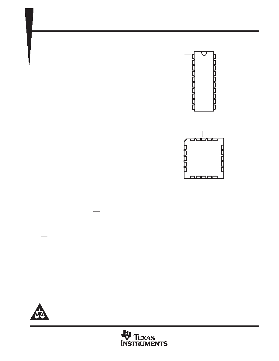
32 1 20 19
910 11 1213
4
5
6
7
8
18
17
16
15
14
2Q
3Q
4Q
5Q
6Q
3D
4D
5D
6D
7D
2D
1D
OE
8Q
7Q
V
1Q
8D
GND
LE
SN54LV573 . . . FK PACKAGE
(TOP VIEW)
CC
SN54LV573 . . . J OR W PACKAGE
SN74LV573 . . . DB, DW, OR PW PACKAGE
(TOP VIEW)
1
2
3
4
5
6
7
8
9
10
20
19
18
17
16
15
14
13
12
11
OE
1D
2D
3D
4D
5D
6D
7D
8D
GND
VCC
1Q
2Q
3Q
4Q
5Q
6Q
7Q
8Q
LE
相关PDF资料 |
PDF描述 |
|---|---|
| SN74LV74ADGV | LV/LV-A/LVX/H SERIES, DUAL POSITIVE EDGE TRIGGERED D FLIP-FLOP, COMPLEMENTARY OUTPUT, PDSO14 |
| SN74LV74ANSE4 | LV/LV-A/LVX/H SERIES, DUAL POSITIVE EDGE TRIGGERED D FLIP-FLOP, COMPLEMENTARY OUTPUT, PDSO14 |
| SN74LV74ANS | LV/LV-A/LVX/H SERIES, DUAL POSITIVE EDGE TRIGGERED D FLIP-FLOP, COMPLEMENTARY OUTPUT, PDSO14 |
| SN74LVC00DR | LVC/LCX/Z SERIES, QUAD 2-INPUT NAND GATE, PDSO14 |
| SN74LVC04DB | LVC/LCX/Z SERIES, HEX 1-INPUT INVERT GATE, PDSO14 |
相关代理商/技术参数 |
参数描述 |
|---|---|
| SN74LV574ADBR | 功能描述:触发器 Octal Edge-Trig D-Ty F-F W/3-State Otpt RoHS:否 制造商:Texas Instruments 电路数量:2 逻辑系列:SN74 逻辑类型:D-Type Flip-Flop 极性:Inverting, Non-Inverting 输入类型:CMOS 输出类型: 传播延迟时间:4.4 ns 高电平输出电流:- 16 mA 低电平输出电流:16 mA 电源电压-最大:5.5 V 最大工作温度:+ 85 C 安装风格:SMD/SMT 封装 / 箱体:X2SON-8 封装:Reel |
| SN74LV574ADBRE4 | 功能描述:触发器 Octal Edge-Trig D-Ty F-F W/3-State Otpt RoHS:否 制造商:Texas Instruments 电路数量:2 逻辑系列:SN74 逻辑类型:D-Type Flip-Flop 极性:Inverting, Non-Inverting 输入类型:CMOS 输出类型: 传播延迟时间:4.4 ns 高电平输出电流:- 16 mA 低电平输出电流:16 mA 电源电压-最大:5.5 V 最大工作温度:+ 85 C 安装风格:SMD/SMT 封装 / 箱体:X2SON-8 封装:Reel |
| SN74LV574ADBRG4 | 功能描述:触发器 Octal Edge Trigred DType FlipFlop RoHS:否 制造商:Texas Instruments 电路数量:2 逻辑系列:SN74 逻辑类型:D-Type Flip-Flop 极性:Inverting, Non-Inverting 输入类型:CMOS 输出类型: 传播延迟时间:4.4 ns 高电平输出电流:- 16 mA 低电平输出电流:16 mA 电源电压-最大:5.5 V 最大工作温度:+ 85 C 安装风格:SMD/SMT 封装 / 箱体:X2SON-8 封装:Reel |
| SN74LV574ADGVR | 功能描述:触发器 Octal Edge-Trig D-Ty F-F W/3-State Otpt RoHS:否 制造商:Texas Instruments 电路数量:2 逻辑系列:SN74 逻辑类型:D-Type Flip-Flop 极性:Inverting, Non-Inverting 输入类型:CMOS 输出类型: 传播延迟时间:4.4 ns 高电平输出电流:- 16 mA 低电平输出电流:16 mA 电源电压-最大:5.5 V 最大工作温度:+ 85 C 安装风格:SMD/SMT 封装 / 箱体:X2SON-8 封装:Reel |
| SN74LV574ADGVRE4 | 功能描述:触发器 Octal Edge-Trig D-Ty F-F W/3-State Otpt RoHS:否 制造商:Texas Instruments 电路数量:2 逻辑系列:SN74 逻辑类型:D-Type Flip-Flop 极性:Inverting, Non-Inverting 输入类型:CMOS 输出类型: 传播延迟时间:4.4 ns 高电平输出电流:- 16 mA 低电平输出电流:16 mA 电源电压-最大:5.5 V 最大工作温度:+ 85 C 安装风格:SMD/SMT 封装 / 箱体:X2SON-8 封装:Reel |
发布紧急采购,3分钟左右您将得到回复。