- 您现在的位置:买卖IC网 > PDF目录373479 > SN74LVC16646ADGVR (Texas Instruments, Inc.) 16-BIT BUS TRANSCEIVER AND REGISTER WITH 3-STATE OUTPUTS PDF资料下载
参数资料
| 型号: | SN74LVC16646ADGVR |
| 厂商: | Texas Instruments, Inc. |
| 英文描述: | 16-BIT BUS TRANSCEIVER AND REGISTER WITH 3-STATE OUTPUTS |
| 中文描述: | 16位总线收发器和登记注册三态输出 |
| 文件页数: | 5/13页 |
| 文件大小: | 184K |
| 代理商: | SN74LVC16646ADGVR |
www.ti.com
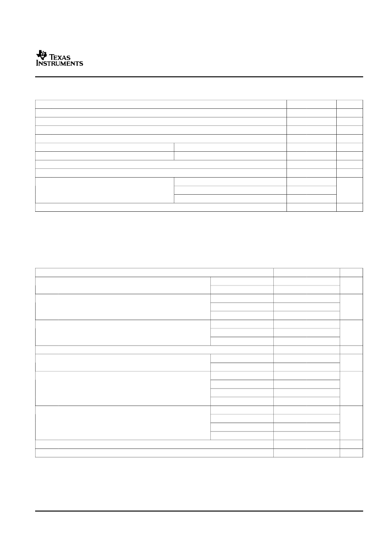
Absolute Maximum Ratings
(1)
over operating free-air temperature range (unless otherwise noted)
Recommended Operating Conditions
(1)
SN74LVC16646A
16-BIT BUS TRANSCEIVER AND REGISTER
WITH 3-STATE OUTPUTS
SCES408B–AUGUST 2002–REVISED APRIL 2005
MIN
–0.5
–0.5
–0.5
–0.5
MAX
6.5
6.5
6.5
UNIT
V
V
V
V
mA
mA
mA
mA
V
CC
V
I
V
O
V
O
I
IK
I
OK
I
O
Supply voltage range
Input voltage range
(2)
Voltage range applied to any output in the high-impedance or power-off state
(2)
Voltage range applied to any output in the high or low state
(2)(3)
Input clamp current
Output clamp current
Continuous output current
Continuous current through each V
CC
or GND
V
CC
+ 0.5
V
I
< 0
V
O
< 0
–50
–50
±50
±100
64
48
56
150
DGG package
DGV package
DL package
θ
JA
Package thermal impedance
(4)
°C/W
T
stg
Storage temperature range
–65
°C
(1)
Stresses beyond those listed under "absolute maximum ratings" may cause permanent damage to the device. These are stress ratings
only, and functional operation of the device at these or any other conditions beyond those indicated under "recommended operating
conditions" is not implied. Exposure to absolute-maximum-rated conditions for extended periods may affect device reliability.
The input negative-voltage and output voltage ratings may be exceeded if the input and output current ratings are observed.
The value of V
is provided in the recommended operating conditions table.
The package thermal impedance is calculated in accordance with JESD 51-7.
(2)
(3)
(4)
MIN
1.65
1.5
MAX
3.6
UNIT
Operating
Data retention only
V
CC
= 1.65 V to 1.95 V
V
CC
= 2.3 V to 2.7 V
V
CC
= 2.7 V to 3.6 V
V
CC
= 1.65 V to 1.95 V
V
CC
= 2.3 V to 2.7 V
V
CC
= 2.7 V to 3.6 V
V
CC
Supply voltage
V
0.65 × V
CC
V
IH
High-level input voltage
1.7
V
2
0.35 × V
CC
V
IL
Low-level input voltage
0.7
0.8
5.5
V
CC
5.5
–4
–8
–12
–24
V
V
I
Input voltage
0
0
0
V
High or low state
3-state
V
CC
= 1.65 V
V
CC
= 2.3 V
V
CC
= 2.7 V
V
CC
= 3 V
V
CC
= 1.65 V
V
CC
= 2.3 V
V
CC
= 2.7 V
V
CC
= 3 V
V
O
Output voltage
V
I
OH
High-level output current
mA
4
8
I
OL
Low-level output current
mA
12
24
10
85
t/
v
T
A
Input transition rise or fall rate
Operating free-air temperature
ns/V
°C
–40
(1)
All unused inputs of the device must be held at V
or GND to ensure proper device operation. Refer to the TI application report,
Implications of Slow or Floating CMOS Inputs
, literature number SCBA004.
5
相关PDF资料 |
PDF描述 |
|---|---|
| SN74LVC1G17DBV3 | SINGLE SCHMITT-TRIGGER BUFFER |
| SN74LVC1G17DCK3 | SINGLE SCHMITT-TRIGGER BUFFER |
| SN74LVC1G17YZTR | SINGLE SCHMITT-TRIGGER BUFFER |
| SN74LVC1G29YEPR | 2-OF-3 DECODER/DEMULTIPLEXER |
| SN74LVC1G57(中文) | CONFIGURABLE MULTIPLE-FUNCTION GATE(可配置的多功能门) |
相关代理商/技术参数 |
参数描述 |
|---|---|
| SN74LVC16646ADL | 功能描述:总线收发器 16B Bus Transceiver And Register RoHS:否 制造商:Fairchild Semiconductor 逻辑类型:CMOS 逻辑系列:74VCX 每芯片的通道数量:16 输入电平:CMOS 输出电平:CMOS 输出类型:3-State 高电平输出电流:- 24 mA 低电平输出电流:24 mA 传播延迟时间:6.2 ns 电源电压-最大:2.7 V, 3.6 V 电源电压-最小:1.65 V, 2.3 V 最大工作温度:+ 85 C 封装 / 箱体:TSSOP-48 封装:Reel |
| SN74LVC16646ADLG4 | 功能描述:总线收发器 16B Bus Transceiver And Register RoHS:否 制造商:Fairchild Semiconductor 逻辑类型:CMOS 逻辑系列:74VCX 每芯片的通道数量:16 输入电平:CMOS 输出电平:CMOS 输出类型:3-State 高电平输出电流:- 24 mA 低电平输出电流:24 mA 传播延迟时间:6.2 ns 电源电压-最大:2.7 V, 3.6 V 电源电压-最小:1.65 V, 2.3 V 最大工作温度:+ 85 C 封装 / 箱体:TSSOP-48 封装:Reel |
| SN74LVC16646ADLR | 功能描述:总线收发器 16BBusTrans Register RoHS:否 制造商:Fairchild Semiconductor 逻辑类型:CMOS 逻辑系列:74VCX 每芯片的通道数量:16 输入电平:CMOS 输出电平:CMOS 输出类型:3-State 高电平输出电流:- 24 mA 低电平输出电流:24 mA 传播延迟时间:6.2 ns 电源电压-最大:2.7 V, 3.6 V 电源电压-最小:1.65 V, 2.3 V 最大工作温度:+ 85 C 封装 / 箱体:TSSOP-48 封装:Reel |
| SN74LVC16646ADLRG4 | 功能描述:总线收发器 16B Bus Transceiver And Register RoHS:否 制造商:Fairchild Semiconductor 逻辑类型:CMOS 逻辑系列:74VCX 每芯片的通道数量:16 输入电平:CMOS 输出电平:CMOS 输出类型:3-State 高电平输出电流:- 24 mA 低电平输出电流:24 mA 传播延迟时间:6.2 ns 电源电压-最大:2.7 V, 3.6 V 电源电压-最小:1.65 V, 2.3 V 最大工作温度:+ 85 C 封装 / 箱体:TSSOP-48 封装:Reel |
| SN74LVC16646DL | 制造商:Rochester Electronics LLC 功能描述:- Bulk 制造商:Texas Instruments 功能描述: |
发布紧急采购,3分钟左右您将得到回复。