- 您现在的位置:买卖IC网 > PDF目录98123 > SN74LVC1G10DCKR (TEXAS INSTRUMENTS INC) LVC/LCX/Z SERIES, 3-INPUT NAND GATE, PDSO6 PDF资料下载
参数资料
| 型号: | SN74LVC1G10DCKR |
| 厂商: | TEXAS INSTRUMENTS INC |
| 元件分类: | 门电路 |
| 英文描述: | LVC/LCX/Z SERIES, 3-INPUT NAND GATE, PDSO6 |
| 封装: | GREEN, PLASTIC, SC-70, 6 PIN |
| 文件页数: | 1/16页 |
| 文件大小: | 721K |
| 代理商: | SN74LVC1G10DCKR |
www.ti.com
FEATURES
DESCRIPTION/ORDERING INFORMATION
SINGLE 3-INPUT POSITIVE-NAND GATE
SCES486D – SEPTEMBER 2003 – REVISED JANUARY 2007
Available in the Texas Instruments
Operation
NanoFree Package
Latch-Up Performance Exceeds 100 mA per
Supports 5-V V
CC Operation
JESD 78, Class II
Inputs Accept Voltages to 5.5 V
ESD Protection Exceeds JESD 22
Max t
pd of 3.8 ns at 3.3 V
–
2000-V Human-Body Model (A114-A)
Low Power Consumption, 10-A Max I
CC
–
200-V Machine Model (A115-A)
±24-mA Output Drive at 3.3 V
–
1000-V Charged Device Model (C101)
I
off Supports Partial-Power-Down Mode
The SN74LVC1G10 performs the Boolean function Y = A
B C or Y = A + B + C in positive logic.
NanoFree package technology is a major breakthrough in IC packaging concepts, using the die as the
package.
This device is fully specified for partial-power-down applications using Ioff. The Ioff circuitry disables the outputs,
preventing damaging current backflow through the device when it is powered down.
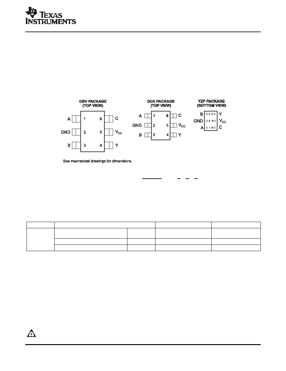
ORDERING INFORMATION
TA
PACKAGE(1)
ORDERABLE PART NUMBER
TOP-SIDE MARKING(2)
NanoFree – WCSP (DSBGA)
Reel of 3000
SN74LVC1G10YZPR
_ _ _C2_
0.23-mm Large Bump – YZP (Pb-free)
–40°C to 85°C
SOT (SOT-23) – DBV
Reel of 3000
SN74LVC1G10DBVR
C10_
SOT (SC-70) – DCK
Reel of 3000
SN74LVC1G10DCKR
C2_
(1)
Package drawings, standard packing quantities, thermal data, symbolization, and PCB design guidelines are available at
www.ti.com/sc/package.
(2)
DBV/DCK: The actual top-side marking has one additional character that designates the assembly/test site.
YZP: The actual top-side marking has three preceding characters to denote year, month, and sequence code, and one following
character to designate the assembly/test site. Pin 1 identifier indicates solder-bump composition (1 = SnPb,
= Pb-free).
Please be aware that an important notice concerning availability, standard warranty, and use in critical applications of Texas
Instruments semiconductor products and disclaimers thereto appears at the end of this data sheet.
NanoFree is a trademark of Texas Instruments.
PRODUCTION DATA information is current as of publication date.
Copyright 2003–2007, Texas Instruments Incorporated
Products conform to specifications per the terms of the Texas
Instruments standard warranty. Production processing does not
necessarily include testing of all parameters.
相关PDF资料 |
PDF描述 |
|---|---|
| SN74LVC1G11DBVRG4 | LVC/LCX/Z SERIES, 3-INPUT AND GATE, PDSO6 |
| SN74LVC1G11DCKRE4 | LVC/LCX/Z SERIES, 3-INPUT AND GATE, PDSO6 |
| SN74LVC1G11DCKREP | LVC/LCX/Z SERIES, 3-INPUT AND GATE, PDSO6 |
| SN74LVC1G11YEPR | LVC/LCX/Z SERIES, 3-INPUT AND GATE, BGA6 |
| SN74LVC1G123YEPR | LVC/LCX/Z SERIES, MONOSTABLE MULTIVIBRATOR, PBGA8 |
相关代理商/技术参数 |
参数描述 |
|---|---|
| SN74LVC1G10DCKR | 制造商:Texas Instruments 功能描述:IC LOGIC NAND GATE SINGLE 3.8NS 6-S 制造商:Texas Instruments 功能描述:IC, LOGIC, NAND GATE, SINGLE, 3.8NS, 6-S |
| SN74LVC1G10DCKRE4 | 功能描述:逻辑门 SNGL 3 Input Pos NAND Gate RoHS:否 制造商:Texas Instruments 产品:OR 逻辑系列:LVC 栅极数量:2 线路数量(输入/输出):2 / 1 高电平输出电流:- 16 mA 低电平输出电流:16 mA 传播延迟时间:3.8 ns 电源电压-最大:5.5 V 电源电压-最小:1.65 V 最大工作温度:+ 125 C 安装风格:SMD/SMT 封装 / 箱体:DCU-8 封装:Reel |
| SN74LVC1G10DCKRG4 | 功能描述:逻辑门 SNGL 3 Input Pos NAND Gate RoHS:否 制造商:Texas Instruments 产品:OR 逻辑系列:LVC 栅极数量:2 线路数量(输入/输出):2 / 1 高电平输出电流:- 16 mA 低电平输出电流:16 mA 传播延迟时间:3.8 ns 电源电压-最大:5.5 V 电源电压-最小:1.65 V 最大工作温度:+ 125 C 安装风格:SMD/SMT 封装 / 箱体:DCU-8 封装:Reel |
| SN74LVC1G10DRYR | 功能描述:逻辑门 Sgl 3-Inp Pos-NAND Gate RoHS:否 制造商:Texas Instruments 产品:OR 逻辑系列:LVC 栅极数量:2 线路数量(输入/输出):2 / 1 高电平输出电流:- 16 mA 低电平输出电流:16 mA 传播延迟时间:3.8 ns 电源电压-最大:5.5 V 电源电压-最小:1.65 V 最大工作温度:+ 125 C 安装风格:SMD/SMT 封装 / 箱体:DCU-8 封装:Reel |
| SN74LVC1G10DSFR | 功能描述:逻辑门 Sgl 3-Inp Pos-NAND Gate RoHS:否 制造商:Texas Instruments 产品:OR 逻辑系列:LVC 栅极数量:2 线路数量(输入/输出):2 / 1 高电平输出电流:- 16 mA 低电平输出电流:16 mA 传播延迟时间:3.8 ns 电源电压-最大:5.5 V 电源电压-最小:1.65 V 最大工作温度:+ 125 C 安装风格:SMD/SMT 封装 / 箱体:DCU-8 封装:Reel |
发布紧急采购,3分钟左右您将得到回复。