- 您现在的位置:买卖IC网 > PDF目录98123 > SN74LVC1G123YEPR (TEXAS INSTRUMENTS INC) LVC/LCX/Z SERIES, MONOSTABLE MULTIVIBRATOR, PBGA8 PDF资料下载
参数资料
| 型号: | SN74LVC1G123YEPR |
| 厂商: | TEXAS INSTRUMENTS INC |
| 元件分类: | 谐振器 |
| 英文描述: | LVC/LCX/Z SERIES, MONOSTABLE MULTIVIBRATOR, PBGA8 |
| 封装: | DSBGA-8 |
| 文件页数: | 1/18页 |
| 文件大小: | 365K |
| 代理商: | SN74LVC1G123YEPR |
www.ti.com
FEATURES
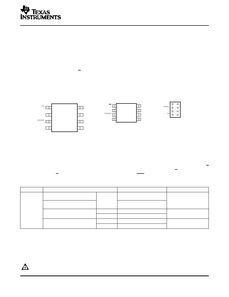
Cext
3
2
5
8
1
A
VCC
B
GND
DCT PACKAGE
(TOP VIEW)
YEP OR YZP PACKAGE
(BOTTOM VIEW)
DCU PACKAGE
(TOP VIEW)
3
2
4
5
1
A
VCC
Rext/Cext
B
GND
B
GND
VCC
Q
CLR
See mechanical drawings for dimensions.
2
5
3
4
8
CLR
Cext
Q
CLR
Rext/Cext
Q
4
6
7
6
7
8
6
1
7
A
Cext
Rext/Cext
DESCRIPTION/ORDERING INFORMATION
SN74LVC1G123
SINGLE RETRIGGERABLE MONOSTABLE MULTIVIBRATOR
WITH SCHMITT-TRIGGER INPUTS
SCES586A – JULY 2004 – REVISED JUNE 2005
Retriggerable for Very Long Output Pulses, up
to 100% Duty Cycle
Available in the Texas Instruments
NanoStar and NanoFree Packages
Overriding Clear Terminates Output Pulse
Supports 5-V VCC Operation
Glitch-Free Power-Up Reset on Outputs
Inputs Accept Voltages to 5.5 V
Ioff Supports Partial-Power-Down Mode
Operation
Max tpd of 8 ns at 3.3 V
Latch-Up Performance Exceeds 100 mA Per
Supports Mixed-Mode Voltage Operation on
JESD 78, Class II
All Ports
ESD Protection Exceeds JESD 22
Schmitt-Trigger Circuitry on A and B Inputs
for Slow Input Transition Rates
– 2000-V Human-Body Model (A114-A)
Edge Triggered From Active-High or
– 200-V Machine Model (A115-A)
Active-Low Gated Logic Inputs
– 1000-V Charged-Device Model (C101)
The SN74LVC1G123 is a single retriggerable monostable multivibrator designed for 1.65-V to 5.5-V VCC
operation.
This monostable multivibrator features output pulse-duration control by three methods. In the first method, the A
input is low, and the B input goes high. In the second method, the B input is high, and the A input goes low. In
the third method, the A input is low, the B input is high, and the clear (CLR) input goes high.
ORDERING INFORMATION
TA
PACKAGE(1)
ORDERABLE PART NUMBER
TOP-SIDE MARKING(2)
NanoStar – WCSP (DSBGA)
SN74LVC1G123YEPR
0.23-mm Large Bump – YEP
Reel of 3000
_ _ _ D8_
NanoFree – WCSP (DSBGA)
SN74LVC1G123YZPR
0.23-mm Large Bump – YZP (Pb-free)
–40
°C to 85°C
Reel of 3000
SN74LVC1G123DCTR
SSOP – DCT
C23_
Reel of 250
SN74LVC1G123DCTT
Reel of 3000
SN74LVC1G123DCUR
VSSOP – DCU
C23_
Reel of 250
SN74LVC1G123DCUT
(1)
Package drawings, standard packing quantities, thermal data, symbolization, and PCB design guidelines are available at
www.ti.com/sc/package.
(2)
DCT: The actual top-side marking has three additional characters that designate the year, month, and assembly/test site.
DCU: The actual top-side marking has one additional character that designates the assembly/test site.
YEP/YZP: The actual top-side marking has three preceding characters to denote year, month, and sequence code, and one following
character to designate the assembly/test site. Pin 1 identifier indicates solder-bump composition (1 = SnPb,
= Pb-free).
Please be aware that an important notice concerning availability, standard warranty, and use in critical applications of Texas
Instruments semiconductor products and disclaimers thereto appears at the end of this data sheet.
NanoStar, NanoFree are trademarks of Texas Instruments.
PRODUCTION DATA information is current as of publication date.
Copyright 2004–2005, Texas Instruments Incorporated
Products conform to specifications per the terms of the Texas
Instruments standard warranty. Production processing does not
necessarily include testing of all parameters.
相关PDF资料 |
PDF描述 |
|---|---|
| SN74LVC1G125YZAR | LVC/LCX/Z SERIES, 1-BIT DRIVER, TRUE OUTPUT, PBGA5 |
| SN74LVC1G126DRLR | LVC/LCX/Z SERIES, 1-BIT DRIVER, TRUE OUTPUT, PDSO5 |
| SN74LVC1G126YEPR | LVC/LCX/Z SERIES, 1-BIT DRIVER, TRUE OUTPUT, PBGA5 |
| SN74LVC1G132DCKT | LVC/LCX/Z SERIES, 2-INPUT NAND GATE, PDSO5 |
| SN74LVC1G132YZPR | LVC/LCX/Z SERIES, 2-INPUT NAND GATE, BGA5 |
相关代理商/技术参数 |
参数描述 |
|---|---|
| SN74LVC1G123YZPR | 功能描述:单稳态多谐振荡器 SNGL Retriggerable Mono Multivibrator RoHS:否 制造商:Texas Instruments 每芯片元件:1 逻辑系列:LVC 逻辑类型:Monostable Multivibrator 封装 / 箱体:SSOP-8 传播延迟时间:18.6 ns 高电平输出电流:- 32 mA 低电平输出电流:32 mA 电源电压-最大:5.5 V 电源电压-最小:1.65 V 最大功率耗散: 最大工作温度:+ 85 C 最小工作温度:- 40 C 封装:Reel |
| SN74LVC1G125DBVR | 功能描述:缓冲器和线路驱动器 SINGLE BUS BUFFER GATE RoHS:否 制造商:Micrel 输入线路数量:1 输出线路数量:2 极性:Non-Inverting 电源电压-最大:+/- 5.5 V 电源电压-最小:+/- 2.37 V 最大工作温度:+ 85 C 安装风格:SMD/SMT 封装 / 箱体:MSOP-8 封装:Reel |
| SN74LVC1G125DBVR | 制造商:Texas Instruments 功能描述:Buffer Gate Logic IC |
| SN74LVC1G125DBVT | 功能描述:缓冲器和线路驱动器 SNGL Bus Buffer Gate RoHS:否 制造商:Micrel 输入线路数量:1 输出线路数量:2 极性:Non-Inverting 电源电压-最大:+/- 5.5 V 电源电压-最小:+/- 2.37 V 最大工作温度:+ 85 C 安装风格:SMD/SMT 封装 / 箱体:MSOP-8 封装:Reel |
| SN74LVC1G125DBVT | 制造商:Texas Instruments 功能描述:GATE LOGIC IC |
发布紧急采购,3分钟左右您将得到回复。