- 您现在的位置:买卖IC网 > PDF目录97706 > SN74LVC843APWLE (TEXAS INSTRUMENTS INC) LVC/LCX/Z SERIES, 9-BIT DRIVER, TRUE OUTPUT, PDSO24 PDF资料下载
参数资料
| 型号: | SN74LVC843APWLE |
| 厂商: | TEXAS INSTRUMENTS INC |
| 元件分类: | 总线收发器 |
| 英文描述: | LVC/LCX/Z SERIES, 9-BIT DRIVER, TRUE OUTPUT, PDSO24 |
| 封装: | TSSOP-24 |
| 文件页数: | 1/10页 |
| 文件大小: | 150K |
| 代理商: | SN74LVC843APWLE |
SN74LVC843A
9-BIT BUS-INTERFACE D-TYPE LATCH
WITH 3-STATE OUTPUTS
SCAS308E – MARCH 1993 – REVISED JUNE 1998
1
POST OFFICE BOX 655303
DALLAS, TEXAS 75265
D EPIC (Enhanced-Performance Implanted
CMOS) Submicron Process
D Typical VOLP (Output Ground Bounce)
< 0.8 V at VCC = 3.3 V, TA = 25°C
D Typical VOHV (Output VOH Undershoot)
> 2 V at VCC = 3.3 V, TA = 25°C
D Power Off Disables Outputs, Permitting
Live Insertion
D Supports Mixed-Mode Signal Operation on
All Ports (5-V Input/Output Voltage With
3.3-V VCC)
D Package Options Include Plastic
Small-Outline (DW), Shrink Small-Outline
(DB), and Thin Shrink Small-Outline (PW)
Packages
description
This 9-bit bus-interface D-type latch is designed for 1.65-V to 3.6-V VCC operation.
The SN74LVC843A is designed specifically for driving highly capacitive or relatively low-impedance loads. It
is particularly suitable for implementing buffer registers, I/O ports, bidirectional bus drivers, and
working registers.
The nine latches are transparent D-type latches. The device has noninverting data (D) inputs and provides true
data at its outputs.
A buffered output-enable (OE) input can be used to place the nine outputs in either a normal logic state (high
or low logic levels) or a high-impedance state. The outputs are also in the high-impedance state during power-up
and power-down conditions. The outputs remain in the high-impedance state while the device is powered down.
In the high-impedance state, the outputs neither load nor drive the bus lines significantly. The high-impedance
state and increased drive provide the capability to drive bus lines without interface or pullup components.
OE does not affect the internal operations of the latch. Previously stored data can be retained or new data can
be entered while the outputs are in the high-impedance state.
Inputs can be driven from either 3.3-V or 5-V devices. This feature allows the use of these devices as translators
in a mixed 3.3-V/5-V system environment.
To ensure the high-impedance state during power up or power down, OE should be tied to VCC through a pullup
resistor; the minimum value of the resistor is determined by the current-sinking capability of the driver.
The SN74LVC843A is characterized for operation from –40
°C to 85°C.
PRODUCT
PREVIEW
Copyright
1998, Texas Instruments Incorporated
PRODUCT PREVIEW information concerns products in the formative or
design phase of development. Characteristic data and other
specifications are design goals. Texas Instruments reserves the right to
change or discontinue these products without notice.
Please be aware that an important notice concerning availability, standard warranty, and use in critical applications of
Texas Instruments semiconductor products and disclaimers thereto appears at the end of this data sheet.
EPIC is a trademark of Texas Instruments Incorporated.
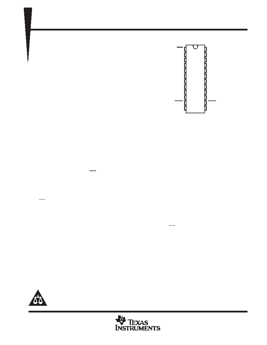
DB, DW, OR PW PACKAGE
(TOP VIEW)
1
2
3
4
5
6
7
8
9
10
11
12
24
23
22
21
20
19
18
17
16
15
14
13
OE
1D
2D
3D
4D
5D
6D
7D
8D
9D
CLR
GND
VCC
1Q
2Q
3Q
4Q
5Q
6Q
7Q
8Q
9Q
PRE
LE
相关PDF资料 |
PDF描述 |
|---|---|
| SN74LVC843PW | LVC/LCX/Z SERIES, 9-BIT DRIVER, TRUE OUTPUT, PDSO24 |
| SN74LVC861DWR | LVC/LCX/Z SERIES, 10-BIT TRANSCEIVER, TRUE OUTPUT, PDSO24 |
| SN74LVCH16241ADGGR | LVC/LCX/Z SERIES, QUAD 4-BIT DRIVER, TRUE OUTPUT, PDSO48 |
| SN74LVCH245PWR | LVC/LCX/Z SERIES, DUAL 4-BIT TRANSCEIVER, TRUE OUTPUT, PDSO20 |
| SN74LVCHR162245ALR | LVC/LCX/Z SERIES, DUAL 8-BIT TRANSCEIVER, TRUE OUTPUT, PDSO48 |
相关代理商/技术参数 |
参数描述 |
|---|---|
| SN74LVC861ADBR | 功能描述:总线收发器 10bit Bus RoHS:否 制造商:Fairchild Semiconductor 逻辑类型:CMOS 逻辑系列:74VCX 每芯片的通道数量:16 输入电平:CMOS 输出电平:CMOS 输出类型:3-State 高电平输出电流:- 24 mA 低电平输出电流:24 mA 传播延迟时间:6.2 ns 电源电压-最大:2.7 V, 3.6 V 电源电压-最小:1.65 V, 2.3 V 最大工作温度:+ 85 C 封装 / 箱体:TSSOP-48 封装:Reel |
| SN74LVC861ADBRE4 | 功能描述:总线收发器 10-Bit Bus Trnscvr With 3-State Outputs RoHS:否 制造商:Fairchild Semiconductor 逻辑类型:CMOS 逻辑系列:74VCX 每芯片的通道数量:16 输入电平:CMOS 输出电平:CMOS 输出类型:3-State 高电平输出电流:- 24 mA 低电平输出电流:24 mA 传播延迟时间:6.2 ns 电源电压-最大:2.7 V, 3.6 V 电源电压-最小:1.65 V, 2.3 V 最大工作温度:+ 85 C 封装 / 箱体:TSSOP-48 封装:Reel |
| SN74LVC861ADBRG4 | 功能描述:总线收发器 10B Bus Transceiver RoHS:否 制造商:Fairchild Semiconductor 逻辑类型:CMOS 逻辑系列:74VCX 每芯片的通道数量:16 输入电平:CMOS 输出电平:CMOS 输出类型:3-State 高电平输出电流:- 24 mA 低电平输出电流:24 mA 传播延迟时间:6.2 ns 电源电压-最大:2.7 V, 3.6 V 电源电压-最小:1.65 V, 2.3 V 最大工作温度:+ 85 C 封装 / 箱体:TSSOP-48 封装:Reel |
| SN74LVC861ADGVR | 功能描述:总线收发器 10bit Bus RoHS:否 制造商:Fairchild Semiconductor 逻辑类型:CMOS 逻辑系列:74VCX 每芯片的通道数量:16 输入电平:CMOS 输出电平:CMOS 输出类型:3-State 高电平输出电流:- 24 mA 低电平输出电流:24 mA 传播延迟时间:6.2 ns 电源电压-最大:2.7 V, 3.6 V 电源电压-最小:1.65 V, 2.3 V 最大工作温度:+ 85 C 封装 / 箱体:TSSOP-48 封装:Reel |
| SN74LVC861ADGVRE4 | 功能描述:总线收发器 Quadruple FET Bus Switch RoHS:否 制造商:Fairchild Semiconductor 逻辑类型:CMOS 逻辑系列:74VCX 每芯片的通道数量:16 输入电平:CMOS 输出电平:CMOS 输出类型:3-State 高电平输出电流:- 24 mA 低电平输出电流:24 mA 传播延迟时间:6.2 ns 电源电压-最大:2.7 V, 3.6 V 电源电压-最小:1.65 V, 2.3 V 最大工作温度:+ 85 C 封装 / 箱体:TSSOP-48 封装:Reel |
发布紧急采购,3分钟左右您将得到回复。