- 您现在的位置:买卖IC网 > PDF目录98132 > SNJ54ABT843W (TEXAS INSTRUMENTS INC) ABT SERIES, 9-BIT DRIVER, TRUE OUTPUT, CDFP24 PDF资料下载
参数资料
| 型号: | SNJ54ABT843W |
| 厂商: | TEXAS INSTRUMENTS INC |
| 元件分类: | 总线收发器 |
| 英文描述: | ABT SERIES, 9-BIT DRIVER, TRUE OUTPUT, CDFP24 |
| 封装: | CERAMIC, DFP-24 |
| 文件页数: | 13/19页 |
| 文件大小: | 593K |
| 代理商: | SNJ54ABT843W |
SN54ABT843, SN74ABT843
9-BIT BUS-INTERFACE D-TYPE LATCHES
WITH 3-STATE OUTPUTS
SCBS197D – FEBRUARY 1991 – REVISED MAY 1997
3
POST OFFICE BOX 655303
DALLAS, TEXAS 75265
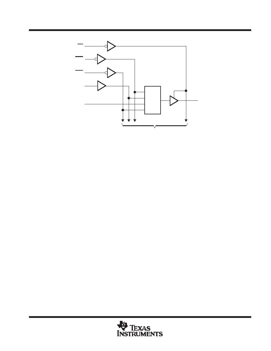
logic diagram (positive logic)
Pin numbers shown are for the DB, DW, JT, NT, and W packages.
1D
OE
PRE
1Q
CLR
LE
To Eight Other Channels
1
14
11
13
2
23
S2
C1
1D
R
absolute maximum ratings over operating free-air temperature range (unless otherwise noted)
Supply voltage range , VCC
–0.5 V to 7 V
. . . . . . . . . . . . . . . . . . . . . . . . . . . . . . . . . . . . . . . . . . . . . . . . . . . . . . . . .
Input voltage range, VI (see Note 1)
–0.5 V to 7 V
. . . . . . . . . . . . . . . . . . . . . . . . . . . . . . . . . . . . . . . . . . . . . . . . . .
Voltage range applied to any output in the high or power-off state, VO
–0.5 V to 5.5 V
. . . . . . . . . . . . . . . . . . .
Current into any output in the low state, IO: SN54ABT843
96 mA
. . . . . . . . . . . . . . . . . . . . . . . . . . . . . . . . . . . . .
SN74ABT843
128 mA
. . . . . . . . . . . . . . . . . . . . . . . . . . . . . . . . . . . . .
Input clamp current, IIK (VI < 0)
–18 mA
. . . . . . . . . . . . . . . . . . . . . . . . . . . . . . . . . . . . . . . . . . . . . . . . . . . . . . . . . . .
Output clamp current, IOK (VO < 0)
–50 mA
. . . . . . . . . . . . . . . . . . . . . . . . . . . . . . . . . . . . . . . . . . . . . . . . . . . . . . . .
Package thermal impedance,
θJA (see Note 2): DB package
104
°C/W
. . . . . . . . . . . . . . . . . . . . . . . . . . . . . . . . .
DW package
81
°C/W
. . . . . . . . . . . . . . . . . . . . . . . . . . . . . . . . .
NT package
67
°C/W
. . . . . . . . . . . . . . . . . . . . . . . . . . . . . . . . . .
Storage temperature range, Tstg
–65
°C to 150°C
. . . . . . . . . . . . . . . . . . . . . . . . . . . . . . . . . . . . . . . . . . . . . . . . . . .
Stresses beyond those listed under “absolute maximum ratings” may cause permanent damage to the device. This is a stress rating only, and
functional operation of the device at these or any other conditions beyond those indicated in the “recommended operating conditions” section of
this specification is not implied. Exposure to absolute-maximum-rated conditions for extended periods may affect device reliability.
NOTES:
1. The input and output negative-voltage ratings may be exceeded if the input and output clamp-current ratings are observed.
2. The package thermal impedance is calculated in accordance with EIA/JEDEC Std JESD51, except for through-hole packages,
which use a trace length of zero.
相关PDF资料 |
PDF描述 |
|---|---|
| SNJ54ABTH182504AHV | ABT SERIES, 20-BIT BOUNDARY SCAN REG TRANSCEIVER, TRUE OUTPUT, CQFP68 |
| SN54ABTH182504AHV | ABT SERIES, 20-BIT BOUNDARY SCAN REG TRANSCEIVER, TRUE OUTPUT, CQFP68 |
| SNJ54AC10W | AC SERIES, TRIPLE 3-INPUT NAND GATE, CDFP14 |
| SN74AC10N | AC SERIES, TRIPLE 3-INPUT NAND GATE, PDIP14 |
| SN74AC10D | AC SERIES, TRIPLE 3-INPUT NAND GATE, PDSO14 |
相关代理商/技术参数 |
参数描述 |
|---|---|
| SNJ54ABT853FK | 制造商:Texas Instruments 功能描述: |
| SNJ54ABT8646FK | 制造商:Texas Instruments 功能描述: |
| SNJ54ABT8646JT | 制造商:Texas Instruments 功能描述:Bus XCVR Single 8-CH 3-ST 28-Pin CDIP Tube 制造商:Rochester Electronics LLC 功能描述:- Tape and Reel |
| SNJ54ABT8652FK | 制造商:TI 制造商全称:Texas Instruments 功能描述:SCAN TEST DEVICES WITH OCTAL BUS TRANSCEIVERS AND REGISTERS |
| SNJ54ABT8652JT | 制造商:TI 制造商全称:Texas Instruments 功能描述:SCAN TEST DEVICES WITH OCTAL BUS TRANSCEIVERS AND REGISTERS |
发布紧急采购,3分钟左右您将得到回复。