- 您现在的位置:买卖IC网 > PDF目录98120 > SNJ54LV367AJ (TEXAS INSTRUMENTS INC) LV/LV-A/LVX/H SERIES, DUAL 4-BIT DRIVER, TRUE OUTPUT, CDIP16 PDF资料下载
参数资料
| 型号: | SNJ54LV367AJ |
| 厂商: | TEXAS INSTRUMENTS INC |
| 元件分类: | 总线收发器 |
| 英文描述: | LV/LV-A/LVX/H SERIES, DUAL 4-BIT DRIVER, TRUE OUTPUT, CDIP16 |
| 封装: | CERAMIC, DIP-16 |
| 文件页数: | 1/18页 |
| 文件大小: | 596K |
| 代理商: | SNJ54LV367AJ |
SN54LV367A, SN74LV367A
HEX BUFFERS AND LINE DRIVERS
WITH 3STATE OUTPUTS
SCLS398G APRIL 1998 REVISED APRIL 2005
1
POST OFFICE BOX 655303
DALLAS, TEXAS 75265
D 2-V to 5.5-V VCC Operation
D Max tpd of 7 ns at 5 V
D Typical VOLP (Output Ground Bounce)
<0.8 V at VCC = 3.3 V, TA = 25°C
D Typical VOHV (Output VOH Undershoot)
>2.3 V at VCC = 3.3 V, TA = 25°C
D Support Mixed-Mode Voltage Operation on
All Ports
D Latch-Up Performance Exceeds 100 mA Per
JESD 78, Class II
D ESD Protection Exceeds JESD 22
2000-V Human-Body Model (A114-A)
200-V Machine Model (A115-A)
1000-V Charged-Device Model (C101)
description/ordering information
The ’LV367A devices are hex buffers and line
drivers designed for 2-V to 5.5-V VCC operation.
These devices are designed specifically to
improve both the performance and density of
3-state memory address drivers, clock drivers,
and bus-oriented receivers and transmitters.
The ’LV367A devices are organized as dual 4-line
and
2-line
buffers/drivers
with
active-low
output-enable (1OE and 2OE) inputs. When OE is
low, the device passes noninverted data from the
A inputs to the Y outputs. When OE is high, the
outputs are in the high-impedance state.
To ensure the high-impedance state during power up or power down, OE should be tied to VCC through a pullup
resistor; the minimum value of the resistor is determined by the current-sinking capability of the driver.
ORDERING INFORMATION
TA
PACKAGE
ORDERABLE
PART NUMBER
TOP-SIDE
MARKING
SOIC D
Tube of 40
SN74LV367AD
LV367A
SOIC D
Reel of 2500
SN74LV367ADR
LV367A
SOP NS
Reel of 2000
SN74LV367ANSR
74LV367A
40
°C to 85°C
SSOP DB
Reel of 2000
SN74LV367ADBR
LV36A
40 C to 85 C
TSSOP PW
Reel of 2000
SN74LV367APWR
LV367A
TSSOP PW
Reel of 250
SN74LV367APWT
LV367A
TVSOP DGV
Reel of 2000
SN74LV367ADGVR
LV367A
CDIP J
Tube of 25
SNJ54LV367AJ
55
°C to 125°C
CFP W
Tube of 150
SNJ54LV367AW
55 C to 125 C
LCCC FK
Tube of 55
SNJ54LV367AFK
Package drawings, standard packing quantities, thermal data, symbolization, and PCB design
guidelines are available at www.ti.com/sc/package.
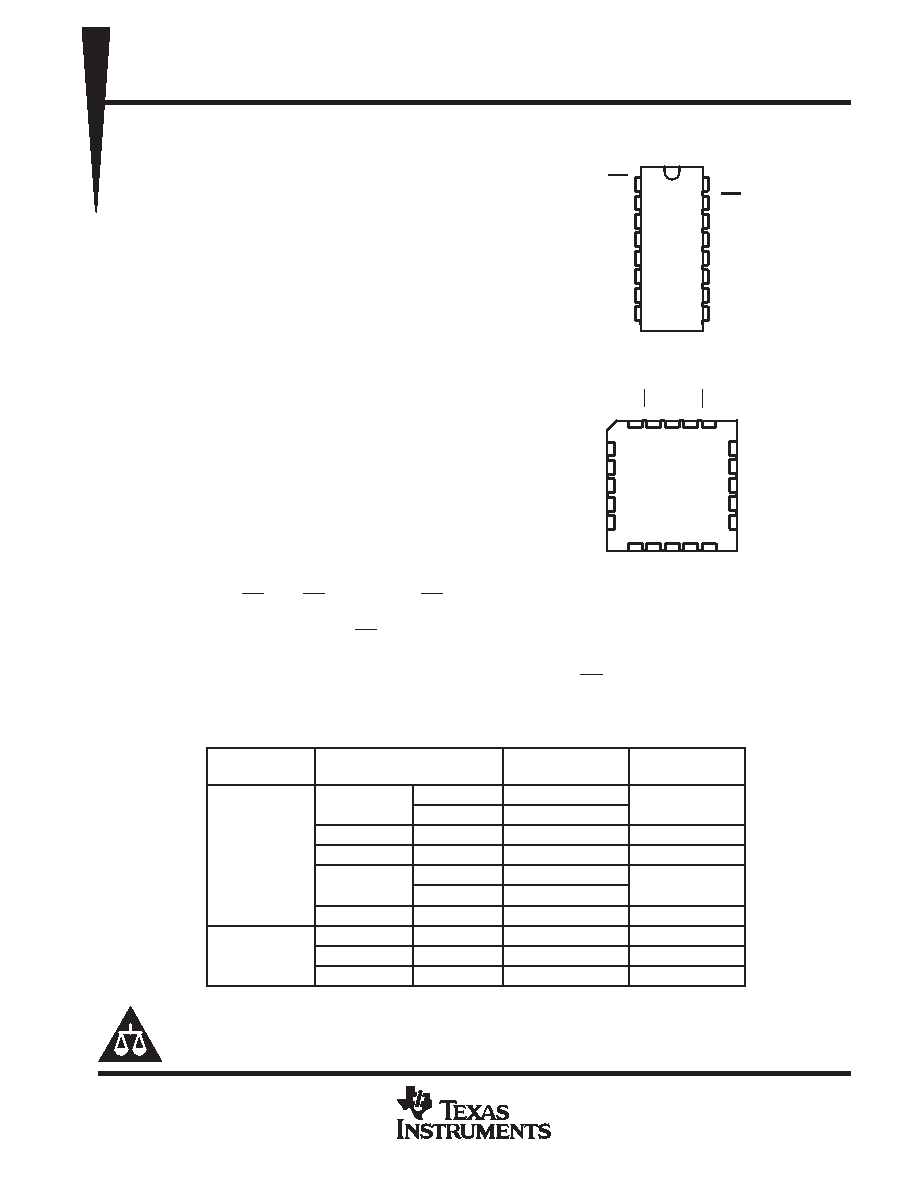
32 1 20 19
910 11 1213
4
5
6
7
8
18
17
16
15
14
2A2
2Y2
NC
2A1
2Y1
1Y1
1A2
NC
1Y2
1A3
1A1
1OE
NC
1Y4
1A4
V
2OE
1Y3
GND
NC
SN54LV367A . . . FK PACKAGE
(TOP VIEW)
CC
NC No internal connection
1
2
3
4
5
6
7
8
16
15
14
13
12
11
10
9
1OE
1A1
1Y1
1A2
1Y2
1A3
1Y3
GND
VCC
2OE
2A2
2Y2
2A1
2Y1
1A4
1Y4
SN54LV367A ...J OR W PACKAGE
SN74LV367A ...D, DB, DGV, NS, OR PW PACKAGE
(TOP VIEW)
UNLESS OTHERWISE NOTED this document contains PRODUCTION
DATA information current as of publication date. Products conform to
specifications per the terms of Texas Instruments standard warranty.
Production processing does not necessarily include testing of all
parameters.
Copyright
2005, Texas Instruments Incorporated
Please be aware that an important notice concerning availability, standard warranty, and use in critical applications of
Texas Instruments semiconductor products and disclaimers thereto appears at the end of this data sheet.
相关PDF资料 |
PDF描述 |
|---|---|
| SN74LV373ADGVRE4 | LV/LV-A/LVX/H SERIES, 8-BIT DRIVER, TRUE OUTPUT, PDSO20 |
| SN74LV373ADWE4 | LV/LV-A/LVX/H SERIES, 8-BIT DRIVER, TRUE OUTPUT, PDSO20 |
| SN74LV373APWRE4 | LV/LV-A/LVX/H SERIES, 8-BIT DRIVER, TRUE OUTPUT, PDSO20 |
| SN74LV373ATNSR | LV/LV-A/LVX/H SERIES, 8-BIT DRIVER, TRUE OUTPUT, PDSO20 |
| SN74LV373ATPW | LV/LV-A/LVX/H SERIES, 8-BIT DRIVER, TRUE OUTPUT, PDSO20 |
相关代理商/技术参数 |
参数描述 |
|---|---|
| SNJ54LVC00AFK | 制造商:Texas Instruments 功能描述: 制造商:Texas Instruments 功能描述:QUADRUPLE 2-INPUT POSITIVE-NAND GATE |
| SNJ54LVC00AJ | 制造商:Texas Instruments 功能描述:5962-9753301QCA, QUAD 2-IN POS-NAND GATE - Rail/Tube |
| SNJ54LVC00AW | 制造商:Texas Instruments 功能描述: |
| SNJ54LVC02AFK | 制造商:Texas Instruments 功能描述: |
| SNJ54LVC02AW | 制造商:Texas Instruments 功能描述:NOR Gate 4-Element 2-IN CMOS 14-Pin CFPAK Tube |
发布紧急采购,3分钟左右您将得到回复。