- 您现在的位置:买卖IC网 > PDF目录98120 > SNJ54LV367AJ (TEXAS INSTRUMENTS INC) LV/LV-A/LVX/H SERIES, DUAL 4-BIT DRIVER, TRUE OUTPUT, CDIP16 PDF资料下载
参数资料
| 型号: | SNJ54LV367AJ |
| 厂商: | TEXAS INSTRUMENTS INC |
| 元件分类: | 总线收发器 |
| 英文描述: | LV/LV-A/LVX/H SERIES, DUAL 4-BIT DRIVER, TRUE OUTPUT, CDIP16 |
| 封装: | CERAMIC, DIP-16 |
| 文件页数: | 11/18页 |
| 文件大小: | 596K |
| 代理商: | SNJ54LV367AJ |
SN54LV367A, SN74LV367A
HEX BUFFERS AND LINE DRIVERS
WITH 3STATE OUTPUTS
SCLS398G APRIL 1998 REVISED APRIL 2005
2
POST OFFICE BOX 655303
DALLAS, TEXAS 75265
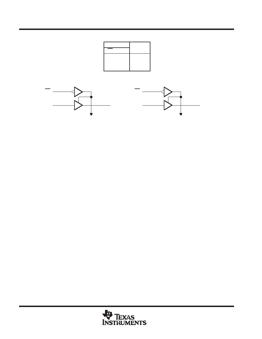
FUNCTION TABLE
(each buffer/driver)
INPUTS
OUTPUT
OE
A
OUTPUT
Y
L
H
L
LL
H
X
Z
logic diagram (positive logic)
1OE
To Three Other Channels
1A1
1Y1
1
23
2OE
To One Other Channel
2A1
2Y1
15
12
11
Pin numbers shown are for the D, DB, DGV, J, NS, PW, and W packages.
absolute maximum ratings over operating free-air temperature range (unless otherwise noted)
Supply voltage range, VCC
0.5 V to 7 V
. . . . . . . . . . . . . . . . . . . . . . . . . . . . . . . . . . . . . . . . . . . . . . . . . . . . . . . . . .
Input voltage range, VI (see Note 1)
0.5 V to 7 V
. . . . . . . . . . . . . . . . . . . . . . . . . . . . . . . . . . . . . . . . . . . . . . . . . .
Voltage range applied to any output in the high-impedance or
power-off state, VO (see Note 1)
0.5 V to 7 V
. . . . . . . . . . . . . . . . . . . . . . . . . . . . . . . . . . . . . . . . . . . . . . . . . . .
Output voltage range applied in the high or low state, VO (see Notes 1 and 2)
0.5 V to VCC + 0.5 V
. . . . . .
Input clamp current, IIK (VI < 0)
20 mA
. . . . . . . . . . . . . . . . . . . . . . . . . . . . . . . . . . . . . . . . . . . . . . . . . . . . . . . . . . .
Output clamp current, IOK (VO < 0)
50 mA
. . . . . . . . . . . . . . . . . . . . . . . . . . . . . . . . . . . . . . . . . . . . . . . . . . . . . . . .
Continuous output current, IO (VO = 0 to VCC)
±35 mA
. . . . . . . . . . . . . . . . . . . . . . . . . . . . . . . . . . . . . . . . . . . . . .
Continuous current through VCC or GND
±70 mA
. . . . . . . . . . . . . . . . . . . . . . . . . . . . . . . . . . . . . . . . . . . . . . . . . . .
Package thermal impedance,
θJA (see Note 3): D package
73
°C/W
. . . . . . . . . . . . . . . . . . . . . . . . . . . . . . . . . . .
DB package
82
°C/W
. . . . . . . . . . . . . . . . . . . . . . . . . . . . . . . . .
DGV package
120
°C/W
. . . . . . . . . . . . . . . . . . . . . . . . . . . . . . .
NS package
64
°C/W
. . . . . . . . . . . . . . . . . . . . . . . . . . . . . . . . .
PW package
108
°C/W
. . . . . . . . . . . . . . . . . . . . . . . . . . . . . . . .
Storage temperature range, Tstg
65
°C to 150°C
. . . . . . . . . . . . . . . . . . . . . . . . . . . . . . . . . . . . . . . . . . . . . . . . . . .
Stresses beyond those listed under “absolute maximum ratings” may cause permanent damage to the device. These are stress ratings only, and
functional operation of the device at these or any other conditions beyond those indicated under “recommended operating conditions” is not
implied. Exposure to absolute-maximum-rated conditions for extended periods may affect device reliability.
NOTES:
1. The input and output negative-voltage ratings may be exceeded if the input and output current ratings are observed.
2. This value is limited to 5.5 V maximum.
3. The package thermal impedance is calculated in accordance with JESD 51-7.
相关PDF资料 |
PDF描述 |
|---|---|
| SN74LV373ADGVRE4 | LV/LV-A/LVX/H SERIES, 8-BIT DRIVER, TRUE OUTPUT, PDSO20 |
| SN74LV373ADWE4 | LV/LV-A/LVX/H SERIES, 8-BIT DRIVER, TRUE OUTPUT, PDSO20 |
| SN74LV373APWRE4 | LV/LV-A/LVX/H SERIES, 8-BIT DRIVER, TRUE OUTPUT, PDSO20 |
| SN74LV373ATNSR | LV/LV-A/LVX/H SERIES, 8-BIT DRIVER, TRUE OUTPUT, PDSO20 |
| SN74LV373ATPW | LV/LV-A/LVX/H SERIES, 8-BIT DRIVER, TRUE OUTPUT, PDSO20 |
相关代理商/技术参数 |
参数描述 |
|---|---|
| SNJ54LVC00AFK | 制造商:Texas Instruments 功能描述: 制造商:Texas Instruments 功能描述:QUADRUPLE 2-INPUT POSITIVE-NAND GATE |
| SNJ54LVC00AJ | 制造商:Texas Instruments 功能描述:5962-9753301QCA, QUAD 2-IN POS-NAND GATE - Rail/Tube |
| SNJ54LVC00AW | 制造商:Texas Instruments 功能描述: |
| SNJ54LVC02AFK | 制造商:Texas Instruments 功能描述: |
| SNJ54LVC02AW | 制造商:Texas Instruments 功能描述:NOR Gate 4-Element 2-IN CMOS 14-Pin CFPAK Tube |
发布紧急采购,3分钟左右您将得到回复。