- 您现在的位置:买卖IC网 > PDF目录271636 > SP574BKS 1-CH 12-BIT SUCCESSIVE APPROXIMATION ADC, PARALLEL ACCESS, PDSO28 PDF资料下载
参数资料
| 型号: | SP574BKS |
| 元件分类: | ADC |
| 英文描述: | 1-CH 12-BIT SUCCESSIVE APPROXIMATION ADC, PARALLEL ACCESS, PDSO28 |
| 封装: | 0.300 INCH, SOIC-28 |
| 文件页数: | 13/15页 |
| 文件大小: | 150K |
| 代理商: | SP574BKS |
SP574B/674B/1674B/774B
12–Bit Sampling A/D Converters
Copyright 2000 Sipex Corporation
7
2
28
STS
DGND
12/8
CS
A0
R/C
CE
THREE–STATE BUFFERS AND CONTROL
NIBBLE A
NIBBLE B
NIBBLE C
27
26
25
24
23
22
21 20
19 18
17 16
OUTPUT BITS
MSB
LSB
3
4
5
6
CONTROL
LOGIC
OSCILLATOR
12–BITS
SAMPLE/HOLD
CDAC
LSB
MSB
OFFSET/GAIN
TRIM NETWORK
REF
AMP
1
15
VLOGIC
+5V
711
VCC
VEE
9
AGND
+15V
N.C.
8
10
VREF
OUT
VREF
IN
R2
100
R1
100K
100K
-15V
+15V
100
10V
IN
20V
IN
BIP
OFF
13
14
12
ANALOG
INPUTS
0TO10V
0TO20V
12–BIT SAR
COMP
STROBE
10F
0.1F
10F
0.1F
+
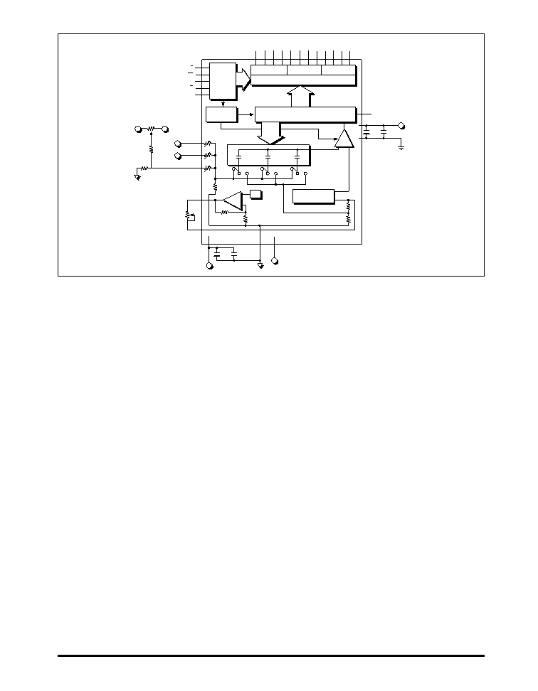
Figure 2. Unipolar Input Connections
signals between ground traces and cross digital
lines at right angles only.
Grounding Considerations
Any ground path from the analog and digital
ground should be as low resistance as possible to
accommodate the ground currents present with
this device.
The analog ground current is approximately
6mA DC while the digital ground is 3mA DC.
The analog and digital common pins should be
tied together as close to the package as possible
to guarantee best performance. The code–de-
pendent currents flow through the V
LOGIC and
V
CC terminals and not through the analog and
digital common pins.
Power Supplies
The supply voltages for the SPx74B must be kept
as quiet as possible from noise pickup and also
regulated from transients or drops. Because the
part has 12–bit accuracy, voltage spikes on the
supply lines can cause several LSB deviations on
the output. Switching power supply noise can be a
problem. Careful filtering and shielding should be
employed to prevent the noise from being picked
up by the converter.
Capacitor bypass pairs are needed from each sup-
ply pin to its respective ground to filter noise and
counter the problems caused by the variations in
supply current. A 10
F tantalum and a 0.1F
ceramic type in parallel between V
LOGIC (pin 1) and
digital common (pin15), and V
CC (pin 7) and
analog common (pin 9) is sufficient. V
EE is gener-
ated internally so pin 11 may be grounded or
connected to a negative supply if the SPx74B is
being used to upgrade an already existing design.
CALIBRATION AND CONNECTION
PROCEDURES
Unipolar
The calibration procedure consists of adjusting the
converter’s most negative output to its ideal value for
offsetadjustment,andthenadjustingthemostpositive
output to its ideal value for gain adjustment.
Starting with offset adjustment and referring to
Figure 2, the midpoint of the first LSB increment
should be positioned at the origin to get an output
code of all 0s. To do this, an input of +1
2 LSB or
+1.22mV for the 10V range and +2.44mV for the
20V range should be applied to the SPx74B.
Adjust the offset potentiometer R
1 for code transi-
tion flickers between 0000 0000 0000 and 0000
0000 0001.
OBSOLETE
-
HIST
ORICAL
REFERENCE
ONL
Y
相关PDF资料 |
PDF描述 |
|---|---|
| SD-14531F3-844K | SYNCHRO OR RESOLVER TO DIGITAL CONVERTER, CDMA36 |
| SD-14531F3-844Z | SYNCHRO OR RESOLVER TO DIGITAL CONVERTER, CDMA36 |
| SD-14590D1-344 | SYNCHRO OR RESOLVER TO DIGITAL CONVERTER, MDIP36 |
| SD-14551DS-182 | SYNCHRO OR RESOLVER TO DIGITAL CONVERTER, CQIP34 |
| SD-14551DS-255 | SYNCHRO OR RESOLVER TO DIGITAL CONVERTER, CQIP34 |
相关代理商/技术参数 |
参数描述 |
|---|---|
| SP574BS | 制造商:SIPEX 制造商全称:Sipex Corporation 功能描述:12-Bit Sampling A/D Converters |
| SP574BT | 制造商:SIPEX 制造商全称:Sipex Corporation 功能描述:12-Bit Sampling A/D Converters |
| SP575 | 制造商:未知厂家 制造商全称:未知厂家 功能描述:低压压扩电路 |
| SP5768 | 制造商:ZARLINK 制造商全称:Zarlink Semiconductor Inc 功能描述:3.0 GHz Low Phase Noise Frequency Synthesiser |
| SP5768KG | 制造商:ZARLINK 制造商全称:Zarlink Semiconductor Inc 功能描述:3.0 GHz Low Phase Noise Frequency Synthesiser |
发布紧急采购,3分钟左右您将得到回复。