- 您现在的位置:买卖IC网 > PDF目录271636 > SP574BKS 1-CH 12-BIT SUCCESSIVE APPROXIMATION ADC, PARALLEL ACCESS, PDSO28 PDF资料下载
参数资料
| 型号: | SP574BKS |
| 元件分类: | ADC |
| 英文描述: | 1-CH 12-BIT SUCCESSIVE APPROXIMATION ADC, PARALLEL ACCESS, PDSO28 |
| 封装: | 0.300 INCH, SOIC-28 |
| 文件页数: | 14/15页 |
| 文件大小: | 150K |
| 代理商: | SP574BKS |
SP574B/674B/1674B/774B
12–Bit Sampling A/D Converters
Copyright 2000 Sipex Corporation
8
+9.9927V for the
±10V range. Adjust the gain
potentiometer R
2 for flicker between codes 1111
1110 and 1111 1111 1111.
Alternative
The 100
potentiometer R
2 provides gain adjust
for 10V and 20V ranges. In some applications, a
full scale of 10.24V (for and LSB of 2.5mV) or
20.48 (for an LSB of 5.0mV) is more convenient.
For these, replace R
2 by a 50, 1% metal film
resistor. Then to provide gain adjust for the 10.24
range, add a 200
potentiometer in series with pin
13. For the 20.48V range, add a 1000
potentiom-
eter in series with pin 14.
The gain adjustment should be done at positive full
scale. The ideal input corresponding to the last
code change is applied. This is 11
2LSB below the
nominal full scale which is +9.9963V for the 10V
range and +19.9927V for the 20V range. Adjust
the gain potentiometer R
2 for flicker between
codes 1111 1111 1110 and 1111 1111 1111. If
calibration is not necessary for the intended appli-
cation, replace R
2 with a 50, 1% metal film
resistor and remove the network analog input to
pin 13 for the 0V to 10V range or to pin 14 for the
0V to 20V range.
Bipolar
The gain and offset errors listed in the specifica-
tions may be adjusted to zero using the potentiom-
eters R
1 and R2 (See Figure 3). If adjustment is not
needed, either or both pots may be replaced by a
50
, 1% metal film resistor.
To calibrate, connect the analog input signal to pin
13 for a
±5V range or to pin 14 for a ±10V range.
First apply a DC input voltage 1
2 LSB above
negative full scale which is –4.9988V for the
±5V
range or –9.9976V for the
±10V range. Adjust the
offset potentiometer R
1 for flicker between output
codes 0000 0000 0000 and 0000 0000 0001. Next,
apply a DC input voltage 11
2 LSB below positive
full scale which is +4.9963V for the
±5 range or
CONTROLLING THE SPx74B
The SPx74B can be operated by most micropro-
cessor systems due to the control input pins and
on–chip logic. It may also be operated in the
“stand–alone” mode and enabled by the R/C
input pin. Full microprocessor control consists
of selecting an 8– or 12–bit conversion cycle,
initiating the conversion, and reading the output
data when ready. The output read has the options
of choosing either 12–bits at once or 8–bits fol-
lowed by 4–bits in a left–justified format. All five
control inputs are TTL/CMOS compatible and
include 12/8, CS, A
0, R/C and CE. The use of these
inputs in controlling the converter’s operation is
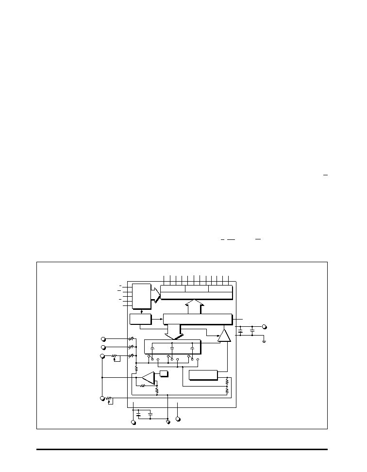
Figure 3. Bipolar Input Connections
2
28
STS
12/8
CS
A0
R/C
CE
THREE–STATE BUFFERS AND CONTROL
NIBBLE A
NIBBLE B
NIBBLE C
27
26
25
24
23
22
21 20
19 18
17 16
OUTPUT BITS
MSB
LSB
3
4
5
6
CONTROL
LOGIC
OSCILLATOR
12–BITS
SAMPLE/HOLD
CDAC
LSB
MSB
OFFSET/GAIN
TRIM NETWORK
REF
AMP
8
10
VREF
OUT
VREF
IN
100
R1
10V
IN
20V
IN
BIP
OFF
13
14
12
ANALOG
INPUTS
12–BIT SAR
COMP
STROBE
100
R2
±5V
±10V
DGND
1
15
VLOGIC
+5V
711
VCC
VEE
9
AGND
+15V
N.C.
10F
0.1F
10F
0.1F
+
OBSOLETE
-
HIST
ORICAL
REFERENCE
ONL
Y
相关PDF资料 |
PDF描述 |
|---|---|
| SD-14531F3-844K | SYNCHRO OR RESOLVER TO DIGITAL CONVERTER, CDMA36 |
| SD-14531F3-844Z | SYNCHRO OR RESOLVER TO DIGITAL CONVERTER, CDMA36 |
| SD-14590D1-344 | SYNCHRO OR RESOLVER TO DIGITAL CONVERTER, MDIP36 |
| SD-14551DS-182 | SYNCHRO OR RESOLVER TO DIGITAL CONVERTER, CQIP34 |
| SD-14551DS-255 | SYNCHRO OR RESOLVER TO DIGITAL CONVERTER, CQIP34 |
相关代理商/技术参数 |
参数描述 |
|---|---|
| SP574BS | 制造商:SIPEX 制造商全称:Sipex Corporation 功能描述:12-Bit Sampling A/D Converters |
| SP574BT | 制造商:SIPEX 制造商全称:Sipex Corporation 功能描述:12-Bit Sampling A/D Converters |
| SP575 | 制造商:未知厂家 制造商全称:未知厂家 功能描述:低压压扩电路 |
| SP5768 | 制造商:ZARLINK 制造商全称:Zarlink Semiconductor Inc 功能描述:3.0 GHz Low Phase Noise Frequency Synthesiser |
| SP5768KG | 制造商:ZARLINK 制造商全称:Zarlink Semiconductor Inc 功能描述:3.0 GHz Low Phase Noise Frequency Synthesiser |
发布紧急采购,3分钟左右您将得到回复。