参数资料
| 型号: | SP6203ER-L/TR |
| 厂商: | Exar Corporation |
| 文件页数: | 3/14页 |
| 文件大小: | 0K |
| 描述: | IC REG LDO ADJ .3A 8DFN |
| 标准包装: | 3,000 |
| 稳压器拓扑结构: | 正,可调式 |
| 输出电压: | 可调至 1.25V |
| 输入电压: | 2.7 V ~ 5.5 V |
| 电压 - 压降(标准): | 0.18V @ 300mA |
| 稳压器数量: | 1 |
| 电流 - 输出: | 300mA |
| 电流 - 限制(最小): | 330mA |
| 工作温度: | -40°C ~ 125°C |
| 安装类型: | 表面贴装 |
| 封装/外壳: | 8-VFDFN 裸露焊盘 |
| 供应商设备封装: | 8-DFN(3x2) |
| 包装: | 带卷 (TR) |
�� �
�
�S� P� 6� 2� 0� 3� /� S� P� 6� 2� 0� 5�
�3� 0� 0� m� A� /� 5� 0� 0� m� A� L� o� w� N� o� i� s� e� C� M� O� S� L� D� O� R� e� g� u� l� a� t� o� r� s�
�Parameter�
�Turn-On� Time� (T� ON� )� 9�
�(from� shutdown� mode)�
�Turn-Off� Time� (T� OFF� )�
�Output� Discharge� Resistance�
�Min.�
�Typ.�
�60�
�100�
�15�
�30�
�Max.�
�120�
�250�
�25�
�Units�
�μS�
�μS�
�?�
�Conditions�
�V� IN� ≥� 4V� 10�
�I� OUT� =� 30mA�
�I� OUT� =� 0.1mA,� V� IN� ≥� 4V� 10�
�I� OUT� =� 300mA,� V� IN� ≥� 4V� 10�
�No� Load�
�Enable� Input� Logic� Low� Voltage�
�Enable� Input� Logic� High� Voltage�
�1.6�
�0.4�
�V�
�V�
�?�
�?�
�Regulator� Shutdown�
�Regulator� Enabled�
�Note� 2:� Output� voltage� temperature� coefficient� is� defined� as� the� worst� case� voltage� change� divided� by� the� total� temperature�
�range.�
�Note� 3:� Regulation� is� measured� at� constant� junction� temperature� using� low� duty� cycle� pulse� testing.� Changes� in� output�
�voltage� due� to� heating� effects� are� covered� by� the� thermal� regulation� specification.�
�Note� 4:� Dropout-voltage� is� defined� as� the� input� to� output� differential� at� which� the� output� voltage� drops� 2%� below� its�
�nominal� value� measured� at� 1V� differential.�
�Note� 5:� Ground� pin� current� is� the� regulator� quiescent� current.� The� total� current� drawn� from� the� supply� is� the� sum� of� the�
�load� current� plus� the� ground� pin� current.�
�Note� 6:� Output� noise� voltage� is� defined� within� a� certain� bandwidth,� namely� 10Hz� <� BW� <� 100kHz.� An� external� bypass� cap�
�(10nF)� from� reference� output� (BYP� pin)� to� ground� significantly� reduces� noise� at� output.�
�Note� 7:� Thermal� regulation� is� defined� as� the� change� in� output� voltage� at� a� time� “t”� after� a� change� in� power� dissipation� is�
�applied,� excluding� load� and� line� regulation� effects.� Specifications� are� for� a� 300mA� load� pulse� at� V� IN� =� 6V� for� t� =� 1ms.�
�Note� 8:� The� wake-up� time� (T� WU� )� is� defined� as� the� time� it� takes� for� the� output� to� start� rising� after� enable� is� brought� high.�
�Note� 9:� The� total� turn-on� time� is� called� the� settling� time� (T� S� ),� which� is� defined� as� the� condition� when� both� the� output� and�
�the� bypass� node� are� within� 2%� of� their� fully� enabled� values� when� released� from� shutdown.�
�Note� 10:� For� output� voltage� versions� requiring� V� IN� to� be� lower� than� 4V,� timing� (T� ON� &� T� OFF� )� increases� slightly.�
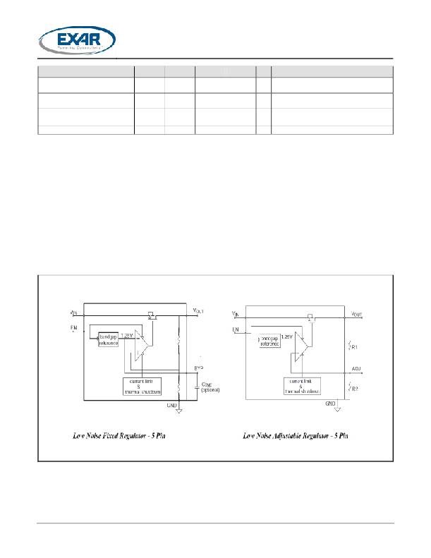
�BLOCK� DIAGRAM�
�Fig.� 2:� SP6203/SP6205� Functional� Diagram�
�?� 2012� Exar� Corporation�
�3/14�
�Rev.� 2.0.0�
�相关PDF资料 |
PDF描述 |
|---|---|
| SP6213EC5-L-2-5 | IC REG LDO 2.5V .1A SC70-5 |
| HSC28DREH-S93 | CONN EDGECARD 56POS .100 EYELET |
| ECC60DRYS-S93 | CONN EDGECARD 120PS DIP .100 SLD |
| EMC28DRTS-S93 | CONN EDGECARD 56POS DIP .100 SLD |
| ECC65DRES-S93 | CONN EDGECARD 130POS .100 EYELET |
相关代理商/技术参数 |
参数描述 |
|---|---|
| SP6205 | 制造商:SIPEX 制造商全称:Sipex Corporation 功能描述:Low Noise, 300mA and 500mA CMOS LDO Regulators |
| SP6205EM5 | 制造商:SIPEX 制造商全称:Sipex Corporation 功能描述:Low Noise, 300mA and 500mA CMOS LDO Regulators |
| SP6205EM5/TR | 制造商:SIPEX 制造商全称:Sipex Corporation 功能描述:Low Noise, 300mA and 500mA CMOS LDO Regulators |
| SP6205EM5-1-8 | 制造商:SIPEX 制造商全称:Sipex Corporation 功能描述:Low Noise, 300mA and 500mA CMOS LDO Regulators |
| SP6205EM5-1-8/TR | 制造商:SIPEX 制造商全称:Sipex Corporation 功能描述:Low Noise, 300mA and 500mA CMOS LDO Regulators |
发布紧急采购,3分钟左右您将得到回复。