参数资料
| 型号: | SP6654EU-L |
| 厂商: | Exar Corporation |
| 文件页数: | 14/17页 |
| 文件大小: | 0K |
| 描述: | IC REG BUCK SYNC ADJ 0.8A 10MSOP |
| 标准包装: | 50 |
| 类型: | 降压(降压) |
| 输出类型: | 可调式 |
| 输出数: | 1 |
| 输出电压: | 1 V ~ 5.5 V |
| 输入电压: | 2.7 V ~ 5.5 V |
| 电流 - 输出: | 800mA |
| 同步整流器: | 是 |
| 工作温度: | -40°C ~ 85°C |
| 安装类型: | 表面贴装 |
| 封装/外壳: | 10-TFSOP,10-MSOP(0.118",3.00mm 宽) |
| 包装: | 管件 |
| 供应商设备封装: | 10-MSOP |
�� �
�
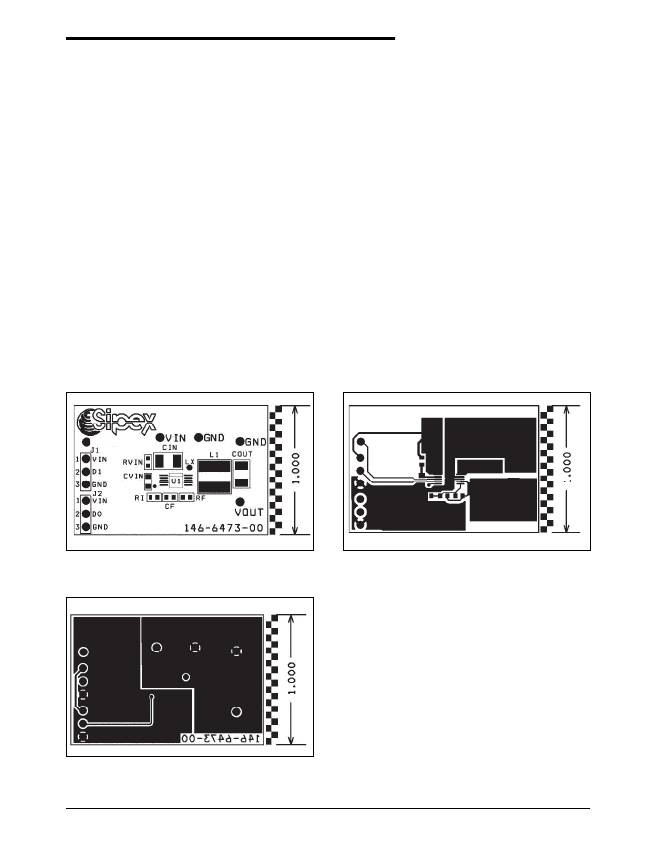
�APPLICATION� INFORMATION�
�the� other� active� components� on� the� board,� some�
�rules� should� be� followed.� Refer� to� the� typical�
�application� schematic� on� page� 1� and� the� sample�
�PCB� layout� shown� in� the� following� figures� to�
�illustrate� how� to� layout� a� SP6654� power� supply.�
�Avoid� injecting� noise� into� the� sensitive� part� of�
�circuit� via� the� ground� plane.� Input� and� output�
�capacitors� conduct� high� frequency� current� through�
�the� ground� plane.� Separate� the� control� and� power�
�grounds� and� connect� them� together� at� a� single�
�point.� Power� ground� plane� is� shown� in� the� figure�
�titled� PCB� top� sample� layout� and� connects� the�
�ground� of� the� C� OUT� capacitor� to� the� ground� of� the�
�C� IN� capacitor� and� then� to� the� PGND� pin� 10.� The�
�control� ground� plane� connects� from� pin� 9� GND� to�
�ground� of� the� C� VIN� capacitor� and� the� R� I� ground�
�return� of� the� feedback� resistor.� These� two� separate�
�control� and� power� ground� planes� come� together� in�
�the� figure� titled� PCB� top� sample� layout� where�
�SP6654� pin� 9� GND� is� connected� to� pin� 10� PGND.�
�SP6654EB�
�PWRGD�
�Figure� 19.� SP6654� PCB� Component� Sample� Layout�
�Figure� 21.� SP6654� PCB� Bottom� Sample� Layout�
�Power� loops� on� the� input� and� output� of� the� con-�
�verter� should� be� laid� out� with� the� shortest� and�
�widest� traces� possible.� The� longer� and� narrower�
�the� trace,� the� higher� the� resistance� and� inductance�
�it� will� have.� The� length� of� traces� in� series� with� the�
�capacitors� increases� its� ESR� and� ESL� and� reduces�
�their� effectiveness� at� high� frequencies.� Therefore,�
�put� the� 1� μ� F� bypass� capacitor� as� close� to� the� V� IN� and�
�GND� pins� of� the� converter� as� possible,� the� 22� μ� F�
�C� IN� close� to� the� P� VIN� pin� and� the� 22� μ� F� output�
�capacitor� as� close� to� the� inductor� as� possible.� The�
�external� voltage� feedback� network� R� F� ,� R� I� and�
�feedforward� capacitor� C� F� should� be� placed� very�
�close� to� the� FB� pin.� Any� noise� traces� like� the� LX�
�pin� should� be� kept� away� from� the� voltage� feedback�
�network� and� separated� from� it� by� using� power�
�ground� copper� to� minimize� EMI.�
�Figure� 20.� SP6654� PCB� Top� Sample� Layout�
�Date:� 2/1/05�
�SP6654� High� Efficiency� 800mA� Synchronous� Buck� Regulator�
�14�
�?� Copyright� 2005� Sipex� Corporation�
�相关PDF资料 |
PDF描述 |
|---|---|
| SP6655ER-L/TR | IC REG BUCK SYNC ADJ 0.4A 10DFN |
| SP6656ER3-L/TR | IC REG BUCK SYNC ADJ 0.4A 10DFN |
| SP6660EP-L | IC REG SWITCHD CAP DBL INV 8PDIP |
| SP6661EU-L/TR | IC REG SWITCHD CAP DBL INV 8MSOP |
| SP6669DEK-L/TRR3 | IC REG BUCK SYNC 1.8V SOT23-5 |
相关代理商/技术参数 |
参数描述 |
|---|---|
| SP6654EU-L/TR | 功能描述:DC/DC 开关控制器 High Eff 800mA Synchronous RoHS:否 制造商:Texas Instruments 输入电压:6 V to 100 V 开关频率: 输出电压:1.215 V to 80 V 输出电流:3.5 A 输出端数量:1 最大工作温度:+ 125 C 安装风格: 封装 / 箱体:CPAK |
| SP6655 | 制造商:SIPEX 制造商全称:Sipex Corporation 功能描述:High Efficiency 400mA Synchronous Buck Regulator Ideal for portable designs powered with Li Ion battery |
| SP6655EB | 功能描述:电源管理IC开发工具 Eval Board for SP6655 Series RoHS:否 制造商:Maxim Integrated 产品:Evaluation Kits 类型:Battery Management 工具用于评估:MAX17710GB 输入电压: 输出电压:1.8 V |
| SP6655ER | 制造商:Rochester Electronics LLC 功能描述: 制造商:Exar Corporation 功能描述: |
| SP6655ER/TR | 制造商:SIPEX 制造商全称:Sipex Corporation 功能描述:High Efficiency 400mA Synchronous Buck Regulator Ideal for portable designs powered with Li Ion battery |
发布紧急采购,3分钟左右您将得到回复。