- 您现在的位置:买卖IC网 > PDF目录193595 > SP7514BN PARALLEL, WORD INPUT LOADING, 2 us SETTLING TIME, 14-BIT DAC, PDSO20 PDF资料下载
参数资料
| 型号: | SP7514BN |
| 元件分类: | DAC |
| 英文描述: | PARALLEL, WORD INPUT LOADING, 2 us SETTLING TIME, 14-BIT DAC, PDSO20 |
| 封装: | 0.300 INCH, SOIC-20 |
| 文件页数: | 6/7页 |
| 文件大小: | 144K |
| 代理商: | SP7514BN |
HS3140/SP7514
HS3140/SP7514 14-Bit Multiplying DACs
Copyright 2000 Sipex Corporation
6
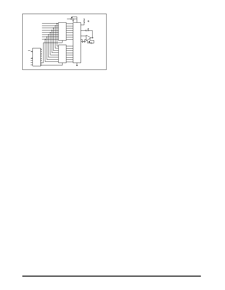
Figure 4. Microprocessor Interface to SP7514/HS3140
D0
D1
D2
D3
D4
D5
D6
D7
CLK
74273
VREF
(+ 25V MAX)
LSB
15
14
13
12
11
10
9
SP7514/
7516
D0
D1
D2
D3
D4
D5
D6
D7
74273
CLK
MSB GND
8
7
6
5
4
3
2
LATCHES
ADDRESS DECODER
G2A
74LS138
G2B
C
B
A
D0
D1
D2
D3
D4
D5
D6
D7
+
–
200
470
3
DD
V
400
WR
BDSEL
A 2
A 1
A 0
VREF
VDD
+
R
I01
I02
UNIPOLAR MODE
(2-QUADRANT)
6
2
3
A1
VOUT
0 TO - V REF
(1-2 - N)
R0S
F
Resistor R
p can be added, this will parallel Rj decreas-
ing the effective resistance. If C
f is reduced the
bandwidth will be increased and settling time de-
creased. However a system penalty for lowering C
f is
to increase noise gain. The trade-off is noise vs.
settling time. If R
p is added then a large value (1F or
greater) non-polarized capacitor C
p should be added
in series with R
p to eliminate any DC drifts. If settling
time is not important, eliminate R
p and Cp, and adjust
C
f to prevent overshoot.
Output Offset
In most applications, the output of the DAC is fed into
an amplifier to convert the DAC’s current output to
voltage. A little known and not commonly discussed
parameteristhelinearityerrorversusoffsetvoltageof
the output amplifier. All CMOS DAC’s must operate
into a virtual ground, i.e., the summing junction of an
opamp.Anyamplifier’soffsetfromtheamplifierwill
appear as an error at the output (which can be related
to LSB’s of error).
MostallCMOSDAC’scurrentlyavailableareimple-
mented using an R-2R ladder network. The formula
for nonlinearity is typically 0.67mV/mV
OS (not de-
rived here). However the SP7516 has a coefficient of
only 0.065mV/mVOS. This is due to the decoding
technique described earlier. CMOS DAC applica-
tions notes (including this one) always show a poten-
tiometer used to null out the amplifier’s offset. If an
amplifier is chosen having ‘pretrimmed’ offset it may
be possible to eliminate this component. Consider the
following calculations:
SP7514/
HS3140
1. Using LF441A amplifier (low power - 741 pinout)
2. Specified offset: 0.5mV max
3. Temperature coefficient of input offset: 10
V/°Cmax
V
OS max (0°C to 70°C)
= 0.5mV + (70
V)10
= 1.2mV
Add'l nonlinearity (max.) = 1.2mV x 0.065mV/mV
=
78
V (1/2 LSB @ 16 Bits)
Where: 78
V = 1/2 LSB @ 16 Bits (10V range)
Via the above configuration, the SP7514/HS3140
can be used to divide an analog signal by digital code
(i.e. for digitally controlled gain). The transfer func-
tion is given in Table 2, where the value of each bit is
0or1.Divisionbyall“0”sisundefinedandcausesthe
op amp to saturate.
Applications Information
Unipolar Operation
Figure 2 shows the interconnections for unipolar
operation. Connect I
O1 and FB1 as shown in diagram.
TieI
O2 (Pin 7), FB3 (Pin 3), and FB4 (Pin 1) to Ground
(Pin8).Asshown,aseriesresistorisrecommendedin
the V
DD supply line to limit current during ‘turn-on’.
To maintain specified linearity, external amplifiers
must be zeroed. Apply an ALL “ZEROES” digital
input and adjust R
OS for VOUT = 0 ± 1mV.
The
SP7514 and HS3140 have been used successfully
with OP-07, OP-27 and LF441A. For high speed
applications the SP2525 is recommended.
Bipolar Operation
Figure 3 shows the interconnections for bipolar op-
eration. Connect I
O1, IO2, FB1, FB3, FB4 as shown in
diagram. Tie LDTR to I
O2. As shown, a series resistor
isrecommendedintheV
DDsupplylinetolimitcurrent
during‘turn-on.Tomaintainspecifiedlinearity,exter-
nal amplifiers must be zeroed. This is best done with
V
REF set to zero and, the DAC register loaded with
10...0 (MSB = 1). Set R
0S1 for V01 = 0. Set R0S2 for
V
OUT = 0. Set VREF to +10V and adjust RB for VOUT
to be 0V.
Grounding
Connect all GND pins to system analog ground
and tie this to digital ground. All unused input pins
must be grounded.
相关PDF资料 |
PDF描述 |
|---|---|
| SP7514JN | PARALLEL, WORD INPUT LOADING, 2 us SETTLING TIME, 14-BIT DAC, PDSO20 |
| SP7514KN | PARALLEL, WORD INPUT LOADING, 2 us SETTLING TIME, 14-BIT DAC, PDSO20 |
| SP7516JN | PARALLEL, WORD INPUT LOADING, 2 us SETTLING TIME, 16-BIT DAC, PDSO24 |
| SP7516AN | PARALLEL, WORD INPUT LOADING, 2 us SETTLING TIME, 16-BIT DAC, PDSO24 |
| SP7516JN | PARALLEL, WORD INPUT LOADING, 2 us SETTLING TIME, 16-BIT DAC, PDSO24 |
相关代理商/技术参数 |
参数描述 |
|---|---|
| SP7514JN | 制造商:SIPEX 制造商全称:Sipex Corporation 功能描述:14-Bit Multiplying DACs |
| SP7514KN | 制造商:SIPEX 制造商全称:Sipex Corporation 功能描述:14-Bit Multiplying DACs |
| SP-75-15 | 功能描述:线性和开关式电源 75W 15V 5A With PFC Function RoHS:否 制造商:TDK-Lambda 产品:Switching Supplies 开放式框架/封闭式:Enclosed 输出功率额定值:800 W 输入电压:85 VAC to 265 VAC 输出端数量:1 输出电压(通道 1):20 V 输出电流(通道 1):40 A 商用/医用: 输出电压(通道 2): 输出电流(通道 2): 安装风格:Rack 长度: 宽度: 高度: |
| SP7516 | 制造商:SIPEX 制造商全称:Sipex Corporation 功能描述:16-Bit Multiplying DACs |
| SP7516AN | 制造商:SIPEX 制造商全称:Sipex Corporation 功能描述:16-Bit Multiplying DACs |
发布紧急采购,3分钟左右您将得到回复。