- 您现在的位置:买卖IC网 > PDF目录271616 > SP7514KN PARALLEL, WORD INPUT LOADING, 2 us SETTLING TIME, 14-BIT DAC, PDSO20 PDF资料下载
参数资料
| 型号: | SP7514KN |
| 元件分类: | DAC |
| 英文描述: | PARALLEL, WORD INPUT LOADING, 2 us SETTLING TIME, 14-BIT DAC, PDSO20 |
| 封装: | 0.300 INCH, SOIC-20 |
| 文件页数: | 4/7页 |
| 文件大小: | 144K |
| 代理商: | SP7514KN |
HS3140/SP7514
HS3140/SP7514 14-Bit Multiplying DACs
Copyright 2000 Sipex Corporation
4
PIN ASSIGNMENTS…
Pin 1 – IO
1 – Current Output 1.
Pin 2 – IO
2 – Current Output 2.
Pin 3 – GND – Ground.
Pin 4 – DB
13 – MSB, Data Bit 1.
Pin 5 – DB
12 – Data Bit 2.
Pin 6 – DB
11 – Data Bit 3.
Pin 7 – DB
10 – Data Bit 4.
Pin 8 – DB
9 – Data Bit 5.
Pin 9 – DB
8 – Data Bit 6.
Pin 10 – DB
7 – Data Bit 7.
Pin 11 – DB
6 – Data Bit 8.
Pin 12 – DB
5 – Data Bit 9.
Pin 13 – DB
4 – Data Bit 10.
Pin 14 – DB
3 – Data Bit 11.
Pin 15 – DB
2 – Data Bit 12.
Pin 16 – DB
1 – Data Bit 13.
Pin 17 – DB
0 – LSB, Data Bit 14.
Pin 18 – V
DD – Positive Supply Voltage.
Pin 19 – V
REF – Reference Voltage Input.
Pin 20 – R
FB – Feedback Resistor.
PRINCIPLES OF OPERATION
TheSP7514/HS3140achievehighaccuracybyusing
a decoded or segmented DAC scheme to implement
this function. The following is a brief description of
this approach.
The most common technique for building a D/A
converter of n bits is to use n switches to turn n current
or voltage sources on or off. The n switches and n
sourcesaredesignedsothateachswitchorbitcontrib-
utestwiceasmuchtotheD/Aconverter’soutputasthe
preceding bit. This technique is commonly known as
binary weighting and allows an n-bit converter to
generate 2n output levels by turning on the proper
combination of bits.
In such binary-weighted converter, the switch
with the smallest contribution (the LSB) accounts
for only 2-n of the converter’s full-scale value.
Similarly, the switch with the largest contribution
(theMSB)accountsfor2-1orhalfoftheconverter’s
full-scale output. Thus it is easy to see that a given
percent change in the MSB will have a greater
effect on the converter’s output than would a
similar percent change in the LSB. For example, a
1% change in the LSB of a 10 bit converter would
only affect the output by 0.001% of full-scale. A
1% change in the MSB of the same converter
would affect the output by 0.5% of FSR.
In order to overcome the problem which results from
the large weighting of the MSB, the two MSB’s can
be decoded to three equally weighted sources. Table
1 shows that all combinations of the two MSB’s of a
converter result in four output levels. So by replacing
the two MSB’s with three bits equally weighted at 1/
4 full-scale and decoding the two MSB digital inputs
into three lines which drive the equally weighted bits,
the same functional performance can be obtained.
ThusbyreplacingthetwoMSBswitchesofaconven-
tional converter with three switches properly de-
coded, the contribution of any switch is reduced from
1/2to1/4.Thisreductioninsensitivityalsoreducesthe
FEATURES…
The SP7514 and HS3140 are precision 14-bit multi-
plying DACs. The DACs are implemented as a one-
chip CMOS circuit with a resistor ladder network.
Three output lines are provided on the DACs to allow
unipolar and bipolar output connection with a mini-
mum of external components. The feedback resistor
is internal. The resistor ladder network termination is
externally available, thus eliminating an external re-
sistor for the 1 LSB offset in bipolar mode.
The SP7514 is available for use in commercial and
industrial temperature ranges, packaged in a 20-pin
SOIC. The HS3140 is available in commercial
and military temperature ranges, packaged in a
20–pin side–brazed DIP. For product processed
and screened to the requirements of MIL–M–
38510 and MIL–STD–883C, please consult the
factory (HS3140B only).
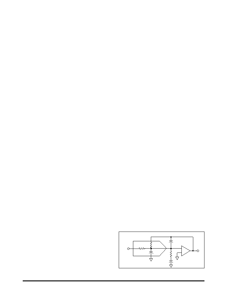
Figure 1. SP7514/HS3140 Equivalent Output Circuit
+
–
EO
Cf
C
Rp
Rf
CO
Ri
VREF
相关PDF资料 |
PDF描述 |
|---|---|
| SD-14621DS-812K | SYNCHRO OR RESOLVER TO DIGITAL CONVERTER, CQIP54 |
| SD-14621DS-812S | SYNCHRO OR RESOLVER TO DIGITAL CONVERTER, CQIP54 |
| SD-14621DS-835 | SYNCHRO OR RESOLVER TO DIGITAL CONVERTER, CQIP54 |
| SD-14595F1-865L | SYNCHRO OR RESOLVER TO DIGITAL CONVERTER, CDFP36 |
| SD-14595F1-865S | SYNCHRO OR RESOLVER TO DIGITAL CONVERTER, CDFP36 |
相关代理商/技术参数 |
参数描述 |
|---|---|
| SP-75-15 | 功能描述:线性和开关式电源 75W 15V 5A With PFC Function RoHS:否 制造商:TDK-Lambda 产品:Switching Supplies 开放式框架/封闭式:Enclosed 输出功率额定值:800 W 输入电压:85 VAC to 265 VAC 输出端数量:1 输出电压(通道 1):20 V 输出电流(通道 1):40 A 商用/医用: 输出电压(通道 2): 输出电流(通道 2): 安装风格:Rack 长度: 宽度: 高度: |
| SP7516 | 制造商:SIPEX 制造商全称:Sipex Corporation 功能描述:16-Bit Multiplying DACs |
| SP7516AN | 制造商:SIPEX 制造商全称:Sipex Corporation 功能描述:16-Bit Multiplying DACs |
| SP7516BN | 制造商:SIPEX 制造商全称:Sipex Corporation 功能描述:16-Bit Multiplying DACs |
| SP7516JN | 制造商:SIPEX 制造商全称:Sipex Corporation 功能描述:16-Bit Multiplying DACs |
发布紧急采购,3分钟左右您将得到回复。