- 您现在的位置:买卖IC网 > PDF目录271616 > SP7514KN PARALLEL, WORD INPUT LOADING, 2 us SETTLING TIME, 14-BIT DAC, PDSO20 PDF资料下载
参数资料
| 型号: | SP7514KN |
| 元件分类: | DAC |
| 英文描述: | PARALLEL, WORD INPUT LOADING, 2 us SETTLING TIME, 14-BIT DAC, PDSO20 |
| 封装: | 0.300 INCH, SOIC-20 |
| 文件页数: | 5/7页 |
| 文件大小: | 144K |
| 代理商: | SP7514KN |
HS3140/SP7514
HS3140/SP7514 14-Bit Multiplying DACs
Copyright 2000 Sipex Corporation
5
2 - 1(MSB)
2 - 2
Output
00
0
1
1/4 Full-Scale
1
0
1/2 Full-Scale
1
3/4 Full-Scale
Table 1. Contribution of the two MSB's
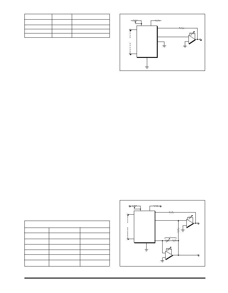
VREF
VDD
470
DIGITAL
INPUTS
RFEEDBACK
I O1
+
-
I O2
GND
ROS
A
V OUT
SP7514
HS3140
200
400
Figure 2. Unipolar Operation
accuracy required of any switch for a given overall
converter accuracy.
With the decoded converter described above, a 1%
change in any of the converter’s switches will affect
the output by no more than 0.25% of full-scale as
compared to 0.5% for a conventional converter. In
other words the conventional D/A converter can be
made less sensitive to the quality of its individual bits
by decoding.
In the SP7514/HS3140 the first four MSB’s are
decodedinto16levelswhichdrive15equallyweighted
current sources. The sensitivity of each switch on the
output is reduced by a factor of 8. Each of the 15
sources contributes 6.25% output change rather than
an MSB change of 50% for the common approach.
FollowingthedecodedsectionoftheDACastandard
binary weighted R-2R approach is used. This divides
each of the 16 levels (or 6.25% of F.S.) into 4096
discrete levels (the 12 LSB’s).
Output Capacitance
The SP7514/HS3140 have very low output capaci-
tance(C
O). This is specified both with all switches ON
andallswitchesOFF.Outputcapacitancevariesfrom
50pF to 100pF over all input codes. This low capaci-
tance is due in part to the decoding technique used.
Smaller switches are used with resulting less capaci-
tance. Three important system characteristics are
affected by C
O and CO; namely digital feedthrough,
settlingtime,andbandwidth.TheDACoutputequiva-
lent circuit can be represented as shown in Figure 1.
Digitalfeedthroughisthechangeinanalogoutputdue
to the toggling conditions on the converter input data
lines when the analog input V
REF is at 0V. The
SP7514/HS3140verylowC
O andthereforewillyield
low digital feedthrough. Inputs to the DAC can be
buffered.Thisinputlatchwithmicroprocessorcontrol
is shown in Figure 4.
SettlingtimeisdirectlyaffectedbyC
O.InFigure1,CO
combines with R
f to add a pole to the open loop
response, reducing bandwidth and causing excessive
phase shift - which could result in ringing and/or
oscillation.Afeedbackcapacitor,C
f must be added to
restore stability. Even with C
f, there is still a zero-pole
mismatch due to R
iCO which is code dependent. This
codedependentmismatchisminimizedwhenC
ORi =
R
fCf. However Cf must now be made larger to
compensate for worst case
R
iCO - resulting in re-
ducedbandwidthandincreasedsettlingtime.Withthe
SP7514/HS3140, small values for C
f must be used.
DIGITAL
INPUTS
RFEEDBACK
I O1
+
-
IO2
GND
ROS1
A
VOUT
1
+
-
A2
ROS2
V OUT1
A1, A2, OP-07
4K
4K
ROS2
R
200
VREF
VDD
470
400
SP7514
HS3140
Figure 3. Bipolar Operation
TRANSFER FUNCTION (N=14)
BINARY INPUT UNIPOLAR OUTPUT BIPOLAR OUTPUT
111...111
–V
REF (1 - 2
–N
)–V
REF (1 – 2
–(N – 1)
)
100...001
–V
REF (1/2 + 2
–N
)–V
REF (2
–(N – 1)
)
100...000
–V
REF /2
0
011...111
–V
REF (1/2 – 2
–N
)V
REF (2
–(N – 1)
)
000…001
–V
REF (2
(N – 1)
)V
REF (1 – 2
–(N – 1)
)
000...000
0
V
REF
Table 2. Transfer Function
相关PDF资料 |
PDF描述 |
|---|---|
| SD-14621DS-812K | SYNCHRO OR RESOLVER TO DIGITAL CONVERTER, CQIP54 |
| SD-14621DS-812S | SYNCHRO OR RESOLVER TO DIGITAL CONVERTER, CQIP54 |
| SD-14621DS-835 | SYNCHRO OR RESOLVER TO DIGITAL CONVERTER, CQIP54 |
| SD-14595F1-865L | SYNCHRO OR RESOLVER TO DIGITAL CONVERTER, CDFP36 |
| SD-14595F1-865S | SYNCHRO OR RESOLVER TO DIGITAL CONVERTER, CDFP36 |
相关代理商/技术参数 |
参数描述 |
|---|---|
| SP-75-15 | 功能描述:线性和开关式电源 75W 15V 5A With PFC Function RoHS:否 制造商:TDK-Lambda 产品:Switching Supplies 开放式框架/封闭式:Enclosed 输出功率额定值:800 W 输入电压:85 VAC to 265 VAC 输出端数量:1 输出电压(通道 1):20 V 输出电流(通道 1):40 A 商用/医用: 输出电压(通道 2): 输出电流(通道 2): 安装风格:Rack 长度: 宽度: 高度: |
| SP7516 | 制造商:SIPEX 制造商全称:Sipex Corporation 功能描述:16-Bit Multiplying DACs |
| SP7516AN | 制造商:SIPEX 制造商全称:Sipex Corporation 功能描述:16-Bit Multiplying DACs |
| SP7516BN | 制造商:SIPEX 制造商全称:Sipex Corporation 功能描述:16-Bit Multiplying DACs |
| SP7516JN | 制造商:SIPEX 制造商全称:Sipex Corporation 功能描述:16-Bit Multiplying DACs |
发布紧急采购,3分钟左右您将得到回复。