- 您现在的位置:买卖IC网 > PDF目录97103 > SP8690BDG (ZARLINK SEMICONDUCTOR INC) 8690 SERIES, PRESCALER, CDIP16 PDF资料下载
参数资料
| 型号: | SP8690BDG |
| 厂商: | ZARLINK SEMICONDUCTOR INC |
| 元件分类: | 谐振器 |
| 英文描述: | 8690 SERIES, PRESCALER, CDIP16 |
| 封装: | CERAMIC, DIP-16 |
| 文件页数: | 3/8页 |
| 文件大小: | 202K |
| 代理商: | SP8690BDG |
2
SP8690/SP8691
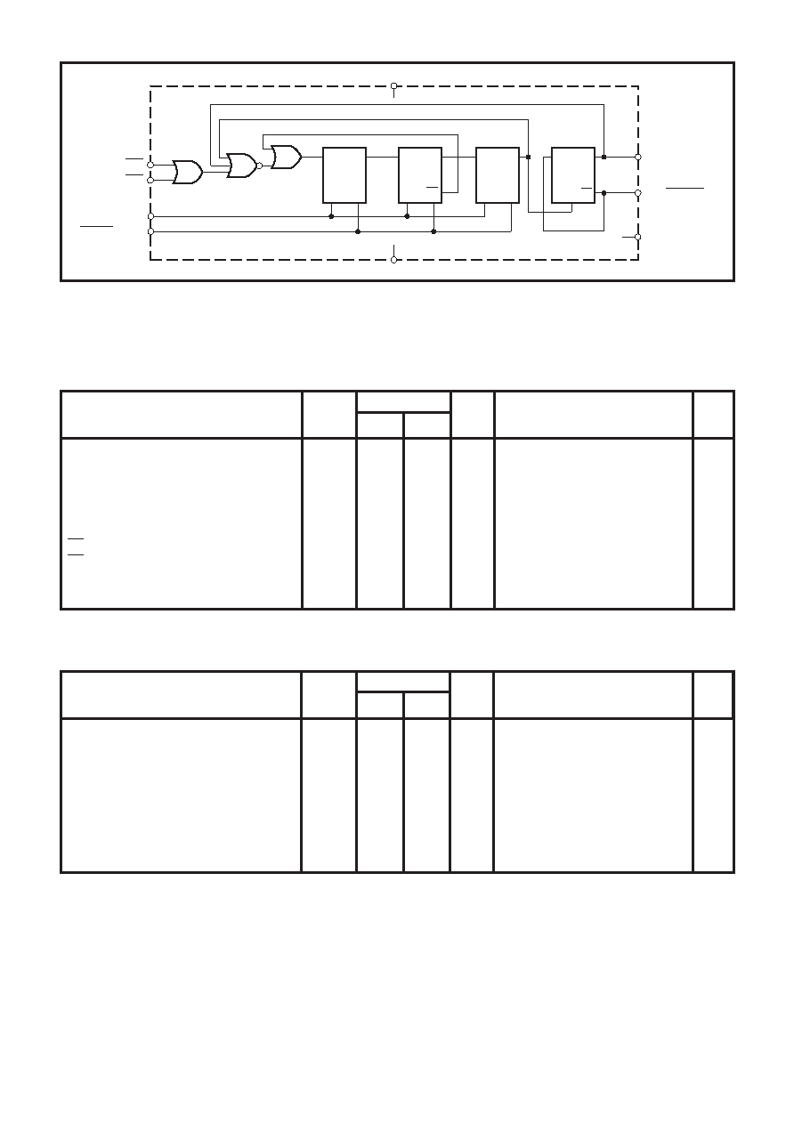
Fig. 3 Functional diagram (SP8691)
Characteristic
Maximum frequency (sinewave input)
Minimum frequency (sinewave input)
Power supply current
ECL output high voltage
ECL output low voltage
PE input high voltage
PE input low voltage
Clock to ECL output delay
Set-up time
Release time
Symbol
fMAX
fMIN
IEE
VOH
VOL
VINH
VINL
tp
ts
tr
200
2
085
2
18
2
093
3
8
Min.
Max.
40
21
2
07
2
15
2
162
9
Units
Input = 400-800mV p-p
VEE = 250V
VEE = 252V (25°C)
Conditions
Notes
MHz
mA
V
ns
5
6
3, 6
4, 6
ELECTRICAL CHARACTERISTICS
Unless otherwise stated, the Electrical Characteristics are guaranteed over specified supply, frequency and temperature range
ECL OPERATION
Supply voltage, VCC = 0V, VEE = 252V 6 025V
Temperature, T
AMB = 255°C to 1125°C (A Grade), 230°C to 170°C (B Grade)
NOTES
1. The temperature coefficients of VOH = 1163mV/°C, VOL = 1094mV/°C and of VIN = 1122mV/°C.
2. The test configuration for dynamic testing is shown in Fig.8
3. The set-up time ts is defined as the minimum time that can elapse between L→H transition of control input and the next L→H clock pulse transition
to ensure that division by the lower modulus is obtained.
4. The release time tr is defined as the minimum time that can elapse between H→L transition of control input and the next L→H clock pulse transition
to ensure that division by the higher modulus is obtained.
5. SP8690/1B tested at 25
°C only.
6. Guaranteed but not tested.
7. The open collector output is not recommended for use at output frequencies above 15MHz. CLOAD ≤ 5pF.
Characteristic
Maximum frequency (sinewave input)
Minimum frequency (sinewave input)
Power supply current
TTL output low voltage
TTL output high voltage
Clock to TTL output high delay,1ve going
Clock to TTL output low delay,2ve going
Set-up time
Release time
Symbol
fMAX
fMIN
IEE
VOL
VOH
tPLH
tPHL
ts
tr
200
375
3
8
Min.
Max.
40
21
05
32
18
Units
Input = 400-800mV p-p
VCC = 50V
VCC = 5V, RL = 560
RL = 560
Conditions
Notes
MHz
mA
V
ns
5
5, 7
6
3, 6
4, 6
TTL OPERATION
Supply voltage, VCC = 5V 6 025V, VEE = 0V
Temperature, T
AMB = 255°C to 1125°C (A Grade), 230°C to 170°C (B Grade)
Value
VCC
D1
Q1
D2
Q2
D3
Q3
D4
Q4
PE1
PE2
CLOCK INPUT
TTL/CMOS
OUTPUT
ECL OUTPUT
Q4
VEE
2
3
1
16
5
12
11
8
9
ECL OUTPUT
Q2
相关PDF资料 |
PDF描述 |
|---|---|
| SP8691ABDG | ECL SERIES, PRESCALER, CDIP16 |
| SP8691ACDG | ECL SERIES, PRESCALER, CDIP16 |
| SP8695ADG | ECL SERIES, PRESCALER, CDIP16 |
| SP8704MP | PRESCALER, PDIP8 |
| SP8706KGMPAS | PRESCALER, PDSO8 |
相关代理商/技术参数 |
参数描述 |
|---|---|
| SP8691 | 制造商:未知厂家 制造商全称:未知厂家 功能描述:200MHz÷8/9/10/11 |
| SP8691AC | 制造商:PSS 功能描述:PRESCALER, 16 Pin, Ceramic, DIP |
| SP8691ADG | 制造商:未知厂家 制造商全称:未知厂家 功能描述:200MHz±8/9/10/11 |
| SP8693AR | 制造商:GEC PLESSEY SEMICONDUCTOR 功能描述: |
| SP8695A | 制造商:未知厂家 制造商全称:未知厂家 功能描述:LOW POWER ECL COUNTER WITH BOTH ECL 10K AND TTL COMPATIBLE OUTPUTS |
发布紧急采购,3分钟左右您将得到回复。