- 您现在的位置:买卖IC网 > PDF目录97103 > SP8690BDG (ZARLINK SEMICONDUCTOR INC) 8690 SERIES, PRESCALER, CDIP16 PDF资料下载
参数资料
| 型号: | SP8690BDG |
| 厂商: | ZARLINK SEMICONDUCTOR INC |
| 元件分类: | 谐振器 |
| 英文描述: | 8690 SERIES, PRESCALER, CDIP16 |
| 封装: | CERAMIC, DIP-16 |
| 文件页数: | 5/8页 |
| 文件大小: | 202K |
| 代理商: | SP8690BDG |
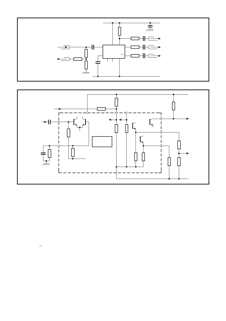
4
SP8690/SP8691
DUT
450
0.1
OUTPUTS TO
SAMPLING
SCOPE
VEE
5
9
8
2
1
16
10n
33
20
INPUT FROM
GENERATOR
INPUT
MONITOR
450
0.1
24k
0.1
VCC
560
11
312
Q4
Fig. 8 Test circuit for dynamic measurements
Fig. 9 Typical application showing interfacing.
OPERATING NOTES
1. The clock inputs can be single or differentially driven. The
clock input is biased internally and is coupled to the signal
source with a suitable capacitor. The input signal path is
completed by an input reference decoupling capacitor which
is connected to ground.
2. In the absence of a signal the device will self-oscillate. If
this is undesirable, it may be prevented by connecting a
68k
resistor from the input to V
EE i.e., from pin 1 or pin 16
to pin 12. This reduces the input sensitiviy by approximately
100mV.
3. The circuit will operate down to DC but slew rate must be
better than 100V/
s.
4. The Q4 and Q4 outputs are compatible with ECLII but can
be interfaced to ECL10K as shown in Fig. 9.
5. The PE inputs are ECLIII/10K compatible and include
internal 10k
pulldown resistors. Unused inputs can therefore
be left open circuit.
6. The input impedance of the SP8690/1 varies as a function
of frequency. See Fig. 7.
7. The TTL/CMOS output is a free collector and the high
state output voltage will depend on the supply that the
collector load is taken to. This should not exceed 12V.
8. The rise/fall time of the open collector output waveform is
directly proportional to load capacitance and load resistor
value. Therefore, load capacitance should be minimised
and the load resistor kept to a minimum consistent with
system power requirements. In the test configuration of Fig.
8 the output rise time is approximately 10ns and the fall time
DIVIDE BY
10/11 (SP8690)
8/9 (SP8691)
9
8
3k
10k
23
8
1
16
5
BIAS
ECL10K
OUTPUT
3k
68k
10n
TTL
CONTROL INPUT
(SEE TRUTH TABLES,
FIGS. 4 AND 5)
10n
3k
91
O/C
CLOCK
INPUT
11
TTL
OUTPUT
36k
15k
560
VCC
VEE
相关PDF资料 |
PDF描述 |
|---|---|
| SP8691ABDG | ECL SERIES, PRESCALER, CDIP16 |
| SP8691ACDG | ECL SERIES, PRESCALER, CDIP16 |
| SP8695ADG | ECL SERIES, PRESCALER, CDIP16 |
| SP8704MP | PRESCALER, PDIP8 |
| SP8706KGMPAS | PRESCALER, PDSO8 |
相关代理商/技术参数 |
参数描述 |
|---|---|
| SP8691 | 制造商:未知厂家 制造商全称:未知厂家 功能描述:200MHz÷8/9/10/11 |
| SP8691AC | 制造商:PSS 功能描述:PRESCALER, 16 Pin, Ceramic, DIP |
| SP8691ADG | 制造商:未知厂家 制造商全称:未知厂家 功能描述:200MHz±8/9/10/11 |
| SP8693AR | 制造商:GEC PLESSEY SEMICONDUCTOR 功能描述: |
| SP8695A | 制造商:未知厂家 制造商全称:未知厂家 功能描述:LOW POWER ECL COUNTER WITH BOTH ECL 10K AND TTL COMPATIBLE OUTPUTS |
发布紧急采购,3分钟左右您将得到回复。