- 您现在的位置:买卖IC网 > PDF目录19292 > SPAKDSP311VL150 (Freescale Semiconductor)IC DSP 24BIT 150MHZ 196-MAPBGA PDF资料下载
参数资料
| 型号: | SPAKDSP311VL150 |
| 厂商: | Freescale Semiconductor |
| 文件页数: | 2/96页 |
| 文件大小: | 0K |
| 描述: | IC DSP 24BIT 150MHZ 196-MAPBGA |
| 标准包装: | 2 |
| 系列: | DSP56K/Symphony |
| 类型: | 定点 |
| 接口: | 主机接口,SSI,SCI |
| 时钟速率: | 150MHz |
| 非易失内存: | ROM(576 B) |
| 芯片上RAM: | 384kB |
| 电压 - 输入/输出: | 3.30V |
| 电压 - 核心: | 1.80V |
| 工作温度: | -40°C ~ 100°C |
| 安装类型: | 表面贴装 |
| 封装/外壳: | 196-LBGA |
| 供应商设备封装: | 196-MAPBGA(15x15) |
| 包装: | 托盘 |
第1页当前第2页第3页第4页第5页第6页第7页第8页第9页第10页第11页第12页第13页第14页第15页第16页第17页第18页第19页第20页第21页第22页第23页第24页第25页第26页第27页第28页第29页第30页第31页第32页第33页第34页第35页第36页第37页第38页第39页第40页第41页第42页第43页第44页第45页第46页第47页第48页第49页第50页第51页第52页第53页第54页第55页第56页第57页第58页第59页第60页第61页第62页第63页第64页第65页第66页第67页第68页第69页第70页第71页第72页第73页第74页第75页第76页第77页第78页第79页第80页第81页第82页第83页第84页第85页第86页第87页第88页第89页第90页第91页第92页第93页第94页第95页第96页
DSP56311 Technical Data, Rev. 8
1-6
Freescale Semiconductor
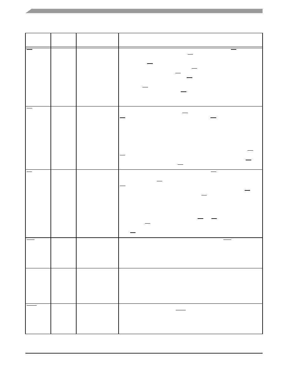
Signals/Connections
BR
Output
Reset: Output
(deasserted)
State during Stop/Wait
depends on BRH bit
setting:
BRH = 0: Output,
deasserted
BRH = 1: Maintains
last state (that is, if
asserted, remains
asserted)
Bus Request—Asserted when the DSP requests bus mastership. BR is deasserted
when the DSP no longer needs the bus. BR may be asserted or deasserted
independently of whether the DSP56311 is a bus master or a bus slave. Bus
“parking” allows BR to be deasserted even though the DSP56311 is the bus master.
(See the description of bus “parking” in the BB signal description.) The bus request
hold (BRH) bit in the BCR allows BR to be asserted under software control even
though the DSP does not need the bus. BR is typically sent to an external bus
arbitrator that controls the priority, parking, and tenure of each master on the same
external bus. BR is affected only by DSP requests for the external bus, never for the
internal bus. During hardware reset, BR is deasserted and the arbitration is reset to
the bus slave state.
BG
Input
Ignored Input
Bus Grant—Asserted by an external bus arbitration circuit when the DSP56311
becomes the next bus master. When BG is asserted, the DSP56311 must wait until
BB is deasserted before taking bus mastership. When BG is deasserted, bus
mastership is typically given up at the end of the current bus cycle. This may occur in
the middle of an instruction that requires more than one external bus cycle for
execution.
The default operation of this bit requires a set-up and hold time as specified in
Chapter 2
. An alternate mode can be invoked: set the asynchronous bus arbitration
enable (ABE) bit (Bit 13) in the Operating Mode Register. When this bit is set, BG and
BB are synchronized internally. This eliminates the respective set-up and hold time
requirements but adds a required delay between the deassertion of an initial BG input
and the assertion of a subsequent BG input.
BB
Input/ Output
Ignored Input
Bus Busy—Indicates that the bus is active. Only after BB is deasserted can the
pending bus master become the bus master (and then assert the signal again). The
bus master may keep BB asserted after ceasing bus activity regardless of whether
BR is asserted or deasserted. Called “bus parking,” this allows the current bus master
to reuse the bus without rearbitration until another device requires the bus. BB is
deasserted by an “active pull-up” method (that is, BB is driven high and then released
and held high by an external pull-up resistor).
The default operation of this signal requires a set-up and hold time as specified in
Chapter 2. An alternative mode can be invoked by setting the ABE bit (Bit 13) in the
Operating Mode Register. When this bit is set, BG and BB are synchronized
internally. See BG for additional information.
Note: BB requires an external pull-up resistor.
CAS
Output
Tri-stated
Column Address Strobe—When the DSP is the bus master, CAS is an active-low
output used by DRAM to strobe the column address. Otherwise, if the Bus
Mastership Enable (BME) bit in the DRAM control register is cleared, the signal is tri-
stated.
Note: DRAM access is not supported above 100 MHz.
BCLK
Output
Tri-stated
Bus Clock
When the DSP is the bus master, BCLK is active when the ATE bit in the Operating
Mode Register is set. When BCLK is active and synchronized to CLKOUT by the
internal PLL, BCLK precedes CLKOUT by one-fourth of a clock cycle.
Note: At operating frequencies above 100 MHz, this signal produces a low-amplitude
waveform that is not usable externally by other devices.
BCLK
Output
Tri-stated
Bus Clock Not
When the DSP is the bus master, BCLK is the inverse of the BCLK signal. Otherwise,
the signal is tri-stated.
Note: At operating frequencies above 100 MHz, this signal produces a low-amplitude
waveform that is not usable externally by other devices.
Table 1-8.
External Bus Control Signals (Continued)
Signal
Name
Type
State During Reset,
Stop, or Wait
Signal Description
相关PDF资料 |
PDF描述 |
|---|---|
| VE-24T-CW-F1 | CONVERTER MOD DC/DC 6.5V 100W |
| VE-24P-CW-F3 | CONVERTER MOD DC/DC 13.8V 100W |
| VE-2TR-CW-F4 | CONVERTER MOD DC/DC 7.5V 100W |
| VI-25B-CY-S | CONVERTER MOD DC/DC 95V 50W |
| TPSD156M025R0100 | CAP TANT 15UF 25V 20% 2917 |
相关代理商/技术参数 |
参数描述 |
|---|---|
| SPAKDSP321VF240 | 功能描述:IC DSP 24BIT 196-MAPBGA RoHS:是 类别:集成电路 (IC) >> 嵌入式 - DSP(数字式信号处理器) 系列:DSP56K/Symphony 标准包装:40 系列:TMS320DM64x, DaVinci™ 类型:定点 接口:I²C,McASP,McBSP 时钟速率:400MHz 非易失内存:外部 芯片上RAM:160kB 电压 - 输入/输出:3.30V 电压 - 核心:1.20V 工作温度:0°C ~ 90°C 安装类型:表面贴装 封装/外壳:548-BBGA,FCBGA 供应商设备封装:548-FCBGA(27x27) 包装:托盘 配用:TMDSDMK642-0E-ND - DEVELPER KIT W/NTSC CAMERA296-23038-ND - DSP STARTER KIT FOR TMS320C6416296-23059-ND - FLASHBURN PORTING KIT296-23058-ND - EVAL MODULE FOR DM642TMDSDMK642-ND - DEVELOPER KIT W/NTSC CAMERA |
| SPAKDSP321VF275 | 功能描述:IC DSP 24BIT 196-MAPBGA RoHS:是 类别:集成电路 (IC) >> 嵌入式 - DSP(数字式信号处理器) 系列:DSP56K/Symphony 标准包装:40 系列:TMS320DM64x, DaVinci™ 类型:定点 接口:I²C,McASP,McBSP 时钟速率:400MHz 非易失内存:外部 芯片上RAM:160kB 电压 - 输入/输出:3.30V 电压 - 核心:1.20V 工作温度:0°C ~ 90°C 安装类型:表面贴装 封装/外壳:548-BBGA,FCBGA 供应商设备封装:548-FCBGA(27x27) 包装:托盘 配用:TMDSDMK642-0E-ND - DEVELPER KIT W/NTSC CAMERA296-23038-ND - DSP STARTER KIT FOR TMS320C6416296-23059-ND - FLASHBURN PORTING KIT296-23058-ND - EVAL MODULE FOR DM642TMDSDMK642-ND - DEVELOPER KIT W/NTSC CAMERA |
| SPAKDSP321VL240 | 功能描述:IC DSP 24BIT 240MHZ 196-MAPBGA RoHS:是 类别:集成电路 (IC) >> 嵌入式 - DSP(数字式信号处理器) 系列:DSP56K/Symphony 标准包装:2 系列:StarCore 类型:SC140 内核 接口:DSI,以太网,RS-232 时钟速率:400MHz 非易失内存:外部 芯片上RAM:1.436MB 电压 - 输入/输出:3.30V 电压 - 核心:1.20V 工作温度:-40°C ~ 105°C 安装类型:表面贴装 封装/外壳:431-BFBGA,FCBGA 供应商设备封装:431-FCPBGA(20x20) 包装:托盘 |
| SPAKDSP321VL275 | 功能描述:IC DSP 24BIT 275MHZ 196-MAPBGA RoHS:是 类别:集成电路 (IC) >> 嵌入式 - DSP(数字式信号处理器) 系列:DSP56K/Symphony 标准包装:40 系列:TMS320DM64x, DaVinci™ 类型:定点 接口:I²C,McASP,McBSP 时钟速率:400MHz 非易失内存:外部 芯片上RAM:160kB 电压 - 输入/输出:3.30V 电压 - 核心:1.20V 工作温度:0°C ~ 90°C 安装类型:表面贴装 封装/外壳:548-BBGA,FCBGA 供应商设备封装:548-FCBGA(27x27) 包装:托盘 配用:TMDSDMK642-0E-ND - DEVELPER KIT W/NTSC CAMERA296-23038-ND - DSP STARTER KIT FOR TMS320C6416296-23059-ND - FLASHBURN PORTING KIT296-23058-ND - EVAL MODULE FOR DM642TMDSDMK642-ND - DEVELOPER KIT W/NTSC CAMERA |
| SPAKDSP56824BU70 | 制造商:Freescale Semiconductor 功能描述: |
发布紧急采购,3分钟左右您将得到回复。