- 您现在的位置:买卖IC网 > PDF目录9613 > SPL505YC256BTT (Silicon Laboratories Inc)IC CLOCK CK505 BEARLAKE 56TSSOP PDF资料下载
参数资料
| 型号: | SPL505YC256BTT |
| 厂商: | Silicon Laboratories Inc |
| 文件页数: | 21/27页 |
| 文件大小: | 0K |
| 描述: | IC CLOCK CK505 BEARLAKE 56TSSOP |
| 标准包装: | 2,000 |
| 类型: | 时钟/频率发生器,多路复用器 |
| PLL: | 是 |
| 主要目的: | Intel CPU,PCI Express(PCIe) |
| 输入: | 晶体 |
| 输出: | LVCMOS |
| 电路数: | 1 |
| 比率 - 输入:输出: | 1:22 |
| 差分 - 输入:输出: | 无/是 |
| 频率 - 最大: | 400MHz |
| 电源电压: | 3.135 V ~ 3.465 V |
| 工作温度: | 0°C ~ 85°C |
| 安装类型: | * |
| 封装/外壳: | * |
| 供应商设备封装: | * |
| 包装: | * |
第1页第2页第3页第4页第5页第6页第7页第8页第9页第10页第11页第12页第13页第14页第15页第16页第17页第18页第19页第20页当前第21页第22页第23页第24页第25页第26页第27页
SPL505YC25
......................Document #: 001-03543 Rev *E Page 3 of 27
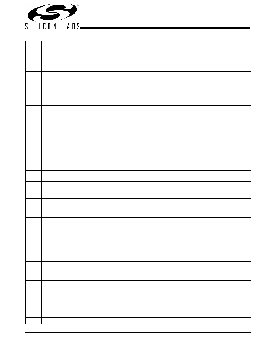
30
SRC5/CPU_STOP#
I/O,
Dif
3.3V tolerant input for stopping CPU outputs/100 MHz Differential serial
reference clocks.
31
VDD_SRC
PWR
3.3V Power supply for SRC PLL.
32
SRC6#
O, DIF 100 MHz Differential serial reference clocks.
33
SRC6
O, DIF 100 MHz Differential serial reference clocks.
34
VSS_SRC
GND
Ground for outputs.
35
SRC7#/OE#_6
I/O,
Dif
100 MHz Differential serial reference clocks/3.3V OE#6 Input controlling
SRC6. Default SRC7.
36
SRC7/OE#_8
I/O,
Dif
100 MHz Differential serial reference clocks/3.3V OE#8 Input controlling
SRC8. Default SRC7.
37
VDD_SRC_IO
PWR
0.7V power supply for SRC outputs.
38
SRC8#/CPUT2_ITP#
O, DIF Selectable differential CPU or SRC clock output. ITP_EN = 0 @ CK_PWRGD
assertion = SRC8
ITP_EN = 1 @ CK_PWRGD assertion = CPU2
Note: CPU2 is an iAMT clock in iAMT mode depending on the configuration set in Byte
11 Bit3:2.
39
SRC8/CPUC2_ITP
O, DIF Selectable differential CPU or SRC clock output. ITP_EN = 0 @ CK_PWRGD
assertion = SRC8
ITP_EN = 1 @ CK_PWRGD assertion = CPU2
Note: CPU2 is an iAMT clock in iAMT mode depending on the configuration set in Byte
11 Bit3:2.
40
IO_VOUT
O
Integrated Linear Regulator Control.
41
VDD_CPU_IO
PWR
0.7V Power supply for CPU outputs.
42
CPU1#
O, DIF Differential CPU clock outputs. Note: CPU1 is an iAMT clock in iAMT mode
depending on the configuration set in Byte 11 Bit3:2.
43
CPU1
O, DIF Differential CPU clock outputs. Note: CPU1 is an iAMT clock in iAMT mode
depending on the configuration set in Byte 11 Bit3:2.
44
VSS_CPU
GND
Ground for outputs.
45
CPU0#
O, DIF Differential CPU clock outputs.
46
CPU0
O, DIF Differential CPU clock outputs.
47
VDD_CPU
PWR
3.3V Power supply for CPU PLL.
48
CK_PWRGD/PWRDWN#
I
3.3V LVTTL input. This pin is a level sensitive strobe used to latch the FS_A,
FS_B, FS_C, FS_D, SRC5_SEL, and ITP_EN.
After CK_PWRGD (active HIGH) assertion, this pin becomes a real-time input
for asserting power down (active LOW).
49
FSB/TEST_MODE
I
3.3V tolerant input for CPU frequency selection.
Selects Ref/N or Tri-state when in test mode
0 = Tri-state, 1 = Ref/N.
Refer to DC Electrical Specifications table for Vil_FS and Vih_FS specifica-
tions.
50
VSS_REF
GND
Ground for outputs.
51
XOUT
O, SE 14.318 MHz Crystal output.
52
XIN
I
14.318 MHz Crystal input.
53
VDD_REF
PWR
3.3V Power supply for outputs and also maintains SMBUS registers during
power-down.
54
REF0/FSC/TEST_SEL
I/O
3.3V tolerant input for CPU frequency selection/fixed 14.318 clock output.
Selects test mode if pulled to VIHFS_C when CK_PWRGD is asserted HIGH.
Refer to DC Electrical Specifications table for VILFS_C, VIMFS_C, VIHFS_C speci-
fications.
55
SMB_DATA
I/O
SMBus compatible SDATA.
56
SMB_CLK
I
SMBus compatible SCLOCK.
Pin Definitions (continued)
Pin No.
Name
Type
Description
相关PDF资料 |
PDF描述 |
|---|---|
| VI-J6V-MW-B1 | CONVERTER MOD DC/DC 5.8V 100W |
| ICL3221CV-T | IC TXRX SGL RS232 3-5.5V 16TSSOP |
| MS3102R14S-11S | CONN RCPT 4POS BOX MNT W/SCKT |
| VI-J40-MW-B1 | CONVERTER MOD DC/DC 5V 100W |
| ICL3221CV | IC TXRX SGL RS232 3-5.5V 16TSSOP |
相关代理商/技术参数 |
参数描述 |
|---|---|
| SPL505YC264BT | 功能描述:时钟发生器及支持产品 CK505 v0.85 RoHS:否 制造商:Silicon Labs 类型:Clock Generators 最大输入频率:14.318 MHz 最大输出频率:166 MHz 输出端数量:16 占空比 - 最大:55 % 工作电源电压:3.3 V 工作电源电流:1 mA 最大工作温度:+ 85 C 安装风格:SMD/SMT 封装 / 箱体:QFN-56 |
| SPL505YC264BTT | 功能描述:时钟发生器及支持产品 CK505 v0.85 RoHS:否 制造商:Silicon Labs 类型:Clock Generators 最大输入频率:14.318 MHz 最大输出频率:166 MHz 输出端数量:16 占空比 - 最大:55 % 工作电源电压:3.3 V 工作电源电流:1 mA 最大工作温度:+ 85 C 安装风格:SMD/SMT 封装 / 箱体:QFN-56 |
| SPL5100PT | 制造商:CHENMKO 制造商全称:Chenmko Enterprise Co. Ltd. 功能描述:SCHOTTKY BARRIER RECTIFIER |
| SPL520LLPT | 制造商:CHENMKO 制造商全称:Chenmko Enterprise Co. Ltd. 功能描述:SCHOTTKY BARRIER RECTIFIER |
| SPL53-1024 | 制造商:Power-One 功能描述: |
发布紧急采购,3分钟左右您将得到回复。