- 您现在的位置:买卖IC网 > PDF目录225223 > SPT1175ACU (FAIRCHILD SEMICONDUCTOR CORP) 1-CH 8-BIT PROPRIETARY METHOD ADC, PARALLEL ACCESS, UUC24 PDF资料下载
参数资料
| 型号: | SPT1175ACU |
| 厂商: | FAIRCHILD SEMICONDUCTOR CORP |
| 元件分类: | ADC |
| 英文描述: | 1-CH 8-BIT PROPRIETARY METHOD ADC, PARALLEL ACCESS, UUC24 |
| 封装: | DIE |
| 文件页数: | 5/8页 |
| 文件大小: | 76K |
| 代理商: | SPT1175ACU |
SPT
5
6/24/97
SPT1175
TYPICAL INTERFACE CIRCUIT
The SPT1175 is an 8-bit analog-to-digital converter which
uses a two-step, ping-pong architecture to perform conver-
sions up to 20 MSPS. Figure 2 shows the typical interface
requirements when using the SPT1175 in normal operation.
The following sections describe the function and operation of
the device.
POWER SUPPLIES AND GROUNDING
The SPT1175 operates from a single +5 V power supply.
AVDD and DVDD must be supplied from the same source
(analog +5 V) to prevent a latch-up condition due to power
supply sequencing. Each power supply pin should be by-
passed as closely as possible to the device. For optimal
performance, both the AGND and DGND should be con-
nected to the system's analog ground plane.
ANALOG INPUT AND VOLTAGE REFERENCE
The SPT1175 input voltage range is VRT>VIN>VRB. Two
reference voltages (VRT and VRB) are required for device
operation. These voltages may be generated externally or
the SPT1175's internal reference may be used.
Inside the SPT1175, reference resistors are placed between
AVDD and VRTS and between AGND and VRBS so that VRTS
and VRBS generate the 2.6 V and 0.6 V references respec-
tively. (See figure 3.) In order to utilize the internal self-bias
reference voltage, VRTS is to be shorted with VRT and the
VRBS pin is to be shorted to the VRB pin. The self-bias internal
reference is not as stable over temperature and supply
variations as externally generated reference voltages but will
perform well in many commercial video applications.
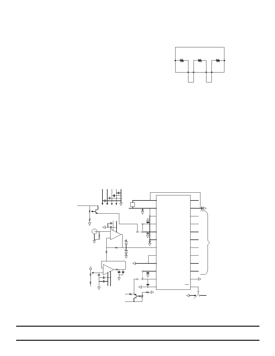
Figure 3 - Reference Circuit Diagram
SPT1175
2.6 V
0.6 V
V
RTS
V
RT
V
RB
V
RBS
AGND
0 V
AVDD
5.0V
DIGITAL INPUTS AND OUTPUTS
The analog input is sampled and tracked on the first 'H' cycle
of the external clock and is held from the falling edge of CLK.
The output remains valid (output hold time), and the new data
becomes valid (output delay time) after the rising edge of
CLK, delayed by 2.5 clock cycles. The clock input and output
enable input must be driven at CMOS-compatible levels.
EVALUATION BOARD
The EB1175 evaluation board is available to aid designers in
demonstrating the full performance of the SPT1175. This
board includes a reference circuit, clock driver circuit, output
data latches, and an on-board reconstruction DAC. An appli-
cation note describing the operation of the board is available.
Contact the factory for price and delivery.
Figure 2 - Typical Interface Circuit
2k
R2
R10
DVDD
AVDD
VRTS
VRT
AVDD
VIN
AGND
VRBS
VRB
DGND
CLK
DVDD
D7
D6
D2
D1
DGND
D3
D4
D5
D0
+5 V
13
14
15
16
17
18
19
20
21
22
23
24
12
11
10(MSB)
9
8
7
6
5
4
3 (LSB)
2
1
+5 V
U1
+
_
-15 +15
C28
C29
U2
+
_
-15
+15
C61
C8
10 k
7.5 k
R6
C58
2
3
-15
VIN
2k
+5
750
R1
R9
Q1
4
7
75
R35
3
2
750
R36
R37
750
6 R15
10
C59
C60
-5
+5
750
R8
Q2
R13
200
OE
FB
D1
D2
U1=Eleantec, EL2030
U2=OP.07
D1=D2=RCA, SK9091
Q1=Q2=2N2222A
FR=FairRite, 2743001111
All capacitors are 0.01 F unless
otherwise specified.
3-ST
+5
EN
Outputs
+15
-15
GND
10
+
10
+5
+15
-15
GND
+
+5
+
-5
+
NOTE: AVDD and DVDD must be supplied from the same source (Analog +5 V)
to prevent a latch-up condition due to power supply sequencing.
相关PDF资料 |
PDF描述 |
|---|---|
| SPT5100 | TRIPLE, 8-BIT DAC, PQFP32 |
| SPT5110SCT | TRIPLE, PARALLEL, 8 BITS INPUT LOADING, 0.027 us SETTLING TIME, 8-BIT DAC, PQFP48 |
| SPT5450SIS | PARALLEL, WORD INPUT LOADING, 0.025 us SETTLING TIME, 14-BIT DAC, PDSO28 |
| SPT574BCJ | 1-CH 12-BIT SUCCESSIVE APPROXIMATION ADC, PARALLEL ACCESS, CDIP28 |
| SPT574CCN | 1-CH 12-BIT SUCCESSIVE APPROXIMATION ADC, PARALLEL ACCESS, PDIP28 |
相关代理商/技术参数 |
参数描述 |
|---|---|
| SPT120301 | 制造商:ITT Interconnect Solutions 功能描述:SPT120301 - Bulk |
| SPT120302 | 制造商:ITT Interconnect Solutions 功能描述:SPT120302 - Bulk |
| SPT-123 | 功能描述:烙铁 COVER ASSEMBLY SP-100T RoHS:否 制造商:Weller 产品:Soldering Stations 类型:Digital, Iron, Stand, Cleaner 瓦特:50 W 最大温度:+ 850 F 电缆类型:US Cord Included |
| SPT-13 | 制造商:Portasol 功能描述:Hot Air Tip and Deflector for 21-14190 and 21-14192 |
| SPT135-1R2L | 制造商:Delta Electronics Inc 功能描述:Ind Power Wirewound 1.2uH 20% 100KHz 34A |
发布紧急采购,3分钟左右您将得到回复。