参数资料
| 型号: | SQ48T15012-NBB0 |
| 厂商: | Power-One |
| 文件页数: | 6/64页 |
| 文件大小: | 0K |
| 描述: | CONV DC-DC 48V IN 1.2V OUT 18W |
| 标准包装: | 25 |
| 系列: | SQ48 |
| 类型: | 隔离 |
| 输出数: | 1 |
| 电压 - 输入(最小): | 36V |
| 电压 - 输入(最大): | 75V |
| Voltage - Output 1: | 1.2V |
| 电流 - 输出(最大): | 15A |
| 电源(瓦) - 制造商系列: | 18W |
| 电压 - 隔离: | 2kV(2000V) |
| 安装类型: | 通孔 |
| 封装/外壳: | 8-DIP 模块,1/4 砖 |
| 尺寸/尺寸: | 2.30" L x 0.90" W x 0.34" H(58.4mm x 22.9mm x 8.6mm) |
| 包装: | 托盘 |
| 工作温度: | -40°C ~ 85°C |
| 电源(瓦特)- 最大: | 18W |
| 其它名称: | 179-2217 SQ48T15012-NAA0 SQ48T15012-NBBO |
第1页第2页第3页第4页第5页当前第6页第7页第8页第9页第10页第11页第12页第13页第14页第15页第16页第17页第18页第19页第20页第21页第22页第23页第24页第25页第26页第27页第28页第29页第30页第31页第32页第33页第34页第35页第36页第37页第38页第39页第40页第41页第42页第43页第44页第45页第46页第47页第48页第49页第50页第51页第52页第53页第54页第55页第56页第57页第58页第59页第60页第61页第62页第63页第64页
�� �
�
�SQ48� DC-DC� Series� Data� Sheet�
�36-75� VDC� Input;� 1.0-12� VDC� Output�
�Test� Conditions�
�All� data� presented� were� taken� with� the� converter�
�soldered� to� a� test� board,� specifically� a� 0.060”� thick�
�printed� wiring� board� (PWB)� with� four� layers.� The� top�
�and� bottom� layers� were� not� metalized.� The� two� inner�
�layers,� comprised� of� two-ounce� copper,� were� used� to�
�provide� traces� for� connectivity� to� the� converter.�
�The� lack� of� metalization� on� the� outer� layers� as� well�
�as� the� limited� thermal� connection� ensured� that� heat�
�transfer� from� the� converter� to� the� PWB� was�
�minimized.� This� provides� a� worst-case� but� consistent�
�scenario� for� thermal� derating� purposes.�
�All� measurements� requiring� airflow� were� made� in� the�
�vertical� and� horizontal� wind� tunnel� using� Infrared� (IR)�
�thermography� and� thermocouples� for� thermometry.�
�Ensuring� components� on� the� converter� do� not�
�exceed� their� ratings� is� important� to� maintaining� high�
�reliability.� If� one� anticipates� operating� the� converter�
�at� or� close� to� the� maximum� loads� specified� in� the�
�derating� curves,� it� is� prudent� to� check� actual�
�operating� temperatures� in� the� application.�
�Thermographic� imaging� is� preferable;� if� this� capability�
�is� not� available,� then� thermocouples� may� be� used.�
�The� use� of� AWG� #40� gauge� thermocouples� is�
�recommended� to� ensure� measurement� accuracy.�
�Careful� routing� of� the� thermocouple� leads� will� further�
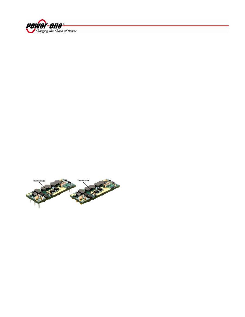
�minimize� measurement� error.� Refer� to� Fig.� E� for� the�
�optimum� measuring� thermocouple� location.�
�Fig.� E:� Location� of� the� thermocouple� for� thermal� testing.�
�Thermal� Derating�
�Load� current� vs.� ambient� temperature� and� airflow�
�rates� are� given� in� Fig.� x.1� to� Fig.� x.4� for� through-hole�
�and� surface-mount� versions.� Ambient� temperature�
�was� varied� between� 25� °C� and� 85� °C,� with� airflow�
�rates� from� 30� to� 500� LFM� (0.15� to� 2.5� m/s),� and�
�vertical� and� horizontal� converter� mounting.�
�For� each� set� of� conditions,� the� maximum� load� current�
�was� defined� as� the� lowest� of:�
�(i)� The� output� current� at� which� any� FET� junction�
�temperature� does� not� exceed� a� maximum� specified�
�temperature� (120°C)� as� indicated� by� the�
�thermographic� image,� or�
�(ii)� The� nominal� rating� of� the� converter� (4� A� on� 12� V,�
�5.3� A� on� 8.0� V,� 8� A� on� 6.0� V,� 10� A� on� 5.0� V,� and� 15� A�
�on� 3.3� –� 1.0� V)).�
�During� normal� operation,� derating� curves� with�
�maximum� FET� temperature� less� or� equal� to� 120� °C�
�should� not� be� exceeded.� Temperature� on� the� PCB� at�
�thermocouple� location� shown� in� Fig.� E� should� not�
�exceed� 118� °C� in� order� to� operate� inside� the� derating�
�curves.�
�Efficiency�
�Fig.� x.5� shows� the� efficiency� vs.� load� current� plot� for�
�ambient� temperature� of� 25� oC,� airflow� rate� of� 300� LFM�
�(1.5� m/s)� with� vertical� mounting� and� input� voltages� of�
�36� V,� 48� V� and� 72� V.� Also,� a� plot� of� efficiency� vs.� load�
�current,� as� a� function� of� ambient� temperature� with�
�Vin� =� 48� V,� airflow� rate� of� 200� LFM� (1� m/s)� with�
�vertical� mounting� is� shown� in� Fig.� x.6.�
�Power� Dissipation�
�Fig.� x.7� shows� the� power� dissipation� vs.� load� current�
�plot� for� Ta� =� 25� oC,� airflow� rate� of� 300� LFM� (1.5� m/s)�
�with� vertical� mounting� and� input� voltages� of� 36� V,� 48�
�V� and� 72� V.� Also,� a� plot� of� power� dissipation� vs.� load�
�current,� as� a� function� of� ambient� temperature� with�
�Vin� =� 48� V,� airflow� rate� of� 200� LFM� (1� m/s)� with�
�vertical� mounting� is� shown� in� Fig.� x.8.�
�Startup�
�Output� voltage� waveforms,� during� the� turn-on�
�transient� using� the� ON/OFF� pin� for� full� rated� load�
�currents� (resistive� load)� are� shown� without� and� with�
�external� load� capacitance� in� Fig.� x.9� and� Fig.� x.10,�
�respectively.�
�Ripple� and� Noise�
�Fig.� x.13� shows� the� output� voltage� ripple� waveform,�
�measured� at� full� rated� load� current� with� a� 10� μF�
�tantalum� and� 1� μF� ceramic� capacitor� across� the�
�output.� Note� that� all� output� voltage� waveforms� are�
�measured� across� a� 1� μF� ceramic� capacitor.�
�The� input� reflected� ripple� current� waveforms� are�
�obtained� using� the� test� setup� shown� in� Fig� x.14.� The�
�corresponding� waveforms� are� shown� in� Fig.� x.15� and�
�Fig.� x.16.�
�SEP� 14,� 2005� revised� to� NOV� 06,� 2006�
�Page� 6� of� 64�
�www.power-one.com�
�相关PDF资料 |
PDF描述 |
|---|---|
| OSTTS12A15A | TERM BLOCK PLUG 7.5MM 12POS |
| OSTTT180181 | TERM BLOCK PLUG 5.0MM 18POS |
| OSTEM107152 | CONN TERM BLOCK 10POS 5MM |
| 74VHC240M | IC INVERTER DUAL 4-INPUT 20SOIC |
| 74HC4060BQ,115 | IC BINARY COUNTER 14ST 16DHVQFN |
相关代理商/技术参数 |
参数描述 |
|---|---|
| SQ48T15012-NBB0G | 制造商:Power-One 功能描述:Module DC-DC 1-OUT 1.2V 15A 50W 8-Pin 1/8-Brick 制造商:Power-One 功能描述:Conn Relay Socket SKT 14 POS Solder ST 制造商:Power-One 功能描述:DC/DC PS SGL-OUT 1.2V 15A 50W - Bulk |
| SQ48T15012-NBBU | 制造商:Power-One 功能描述: |
| SQ48T15012-NDB0 | 功能描述:DC/DC转换器 RoHS:否 制造商:Murata 产品: 输出功率: 输入电压范围:3.6 V to 5.5 V 输入电压(标称): 输出端数量:1 输出电压(通道 1):3.3 V 输出电流(通道 1):600 mA 输出电压(通道 2): 输出电流(通道 2): 安装风格:SMD/SMT 封装 / 箱体尺寸: |
| SQ48T15012-NDB0G | 制造商:Power-One 功能描述:DC/DC PS SGL-OUT 1.2V 15A 50W - Bulk |
| SQ48T15012-PBA0 | 制造商:Power-One 功能描述:DC/DC PS SGL-OUT 1.2V 15A 50W - Bulk |
发布紧急采购,3分钟左右您将得到回复。