- 您现在的位置:买卖IC网 > PDF目录10199 > SSM2160SZ (Analog Devices Inc)IC BALANCE/VOL CTRL DGITL 24SOIC PDF资料下载
参数资料
| 型号: | SSM2160SZ |
| 厂商: | Analog Devices Inc |
| 文件页数: | 2/16页 |
| 文件大小: | 0K |
| 描述: | IC BALANCE/VOL CTRL DGITL 24SOIC |
| 产品变化通告: | Product Discontinuance 27/Oct/2011 |
| 标准包装: | 31 |
| 类型: | 立体声音量控制 |
| 应用: | 解码器,接收器,环绕系统 |
| 安装类型: | 表面贴装 |
| 封装/外壳: | 24-SOIC(0.295",7.50mm 宽) |
| 供应商设备封装: | 24-SOIC W |
| 包装: | 管件 |
| 产品目录页面: | 775 (CN2011-ZH PDF) |
REV. A
–10–
SSM2160
Serial Data Input Format
The standard format for data sent to SSM2160 is an address
byte followed by a data byte. This is depicted in the truth table,
Figure 7. Two 8-bit bytes are required for each master and each
of the six channel updates. The first byte sent contains the address
and is identified by the MSB being logic high. The second byte
contains the data and is identified by the MSB being logic low.
The seven LSBs of the first data byte set the attenuation level
from 0 dB to –127 dB for the master. The five LSBs of the byte
set the channel gain levels from 0 dB to 31 dB.
Serial Data Control Inputs
The SSM2160 provides a simple 3-wire or 4-wire serial inter-
face—see the timing diagram in Figure 1. Data is presented to
the DATA pin and the serial clock to the CLK pin. Data may
be shifted in at rates up to 1 MHz (typically).
The shift register, CLK, is enabled when the
WRITE input is
low. The
WRITE thus serves as a chip select input; however, the
shift register contents are not transferred to the holding register
until the rising edge of
LD. In most cases, WRITE and LD will
be tied together, forming a traditional 3-wire serial interface.
To enable a data transfer, the
WRITE and LD inputs are driven
logic low. The 8-bit serial data, formatted MSB first, is input on
the DATA pin and clocked into the shift register on the falling
edge of CLK. The data is latched on the rising edge of
WRITE
and
LD.
Table III. Input/Output Levels vs. Attenuation/Gain
Input
Gain/Loss
Output
dBu
mV rms Master
Channel
Net
dBu
mV rms
0
775
–31
31
0
775
–31
22
0
31
0
775
–28
31
0
31
3
1100
Saturation Prevention
Unlike a passive potentiometer, the SSM2160 can give up to 31 dB
of gain, thereby creating a potential for saturating the VCAs,
resulting in an undesirable clipping or overload condition. Care-
ful choice of input signal levels and digital gain parameters will
eliminate the possibility. A few of the many acceptable gain and
attenuation settings that keep the signals within the prescribed
limits are shown in Table III. The input and output levels are
given in mV rms and dBu (0 dBu = 0.775 V rms).
Line one of the table: the master is not allowed to have less than
–31 dB attenuation, and the channel is allowed +31 dB of gain.
Since the net gain is zero, there is no possibility of overload with
the expected maximum input signal.
Line two of the table shows that input signal limited to –31 dBu
will allow +31 dB of channel gain and 0 dB of master attenuation.
With an input below –31 dBu, the output will never exceed
0dBu, so no overloading is possible.
Line three of the table allows an input of –28 dBu, master
attenuation of 0 dB, and 31 dB channel gain. The output is a
maximum of 3 dBu (1.1 V rms), which is acceptable for power
supplies of
±6 V or more. So long as V p-p < V
SUPPLY/4, there
will be no overloading (see Table I).
If unity overall gain is required from the SSM2160, there should
be no net gain between the master (loss) and channel (gain), with
both at their lowest attenuation position. Minimum channel gain
is recommended for minimum distortion.
MASTER
DAC
CHANNEL
DAC
IN
OUT
RC
IFS SET
SUMMATION
RESISTOR
R
i
SIGNAL
V+
RM
C
RM, RC, C
EXTERNAL
SSM2160
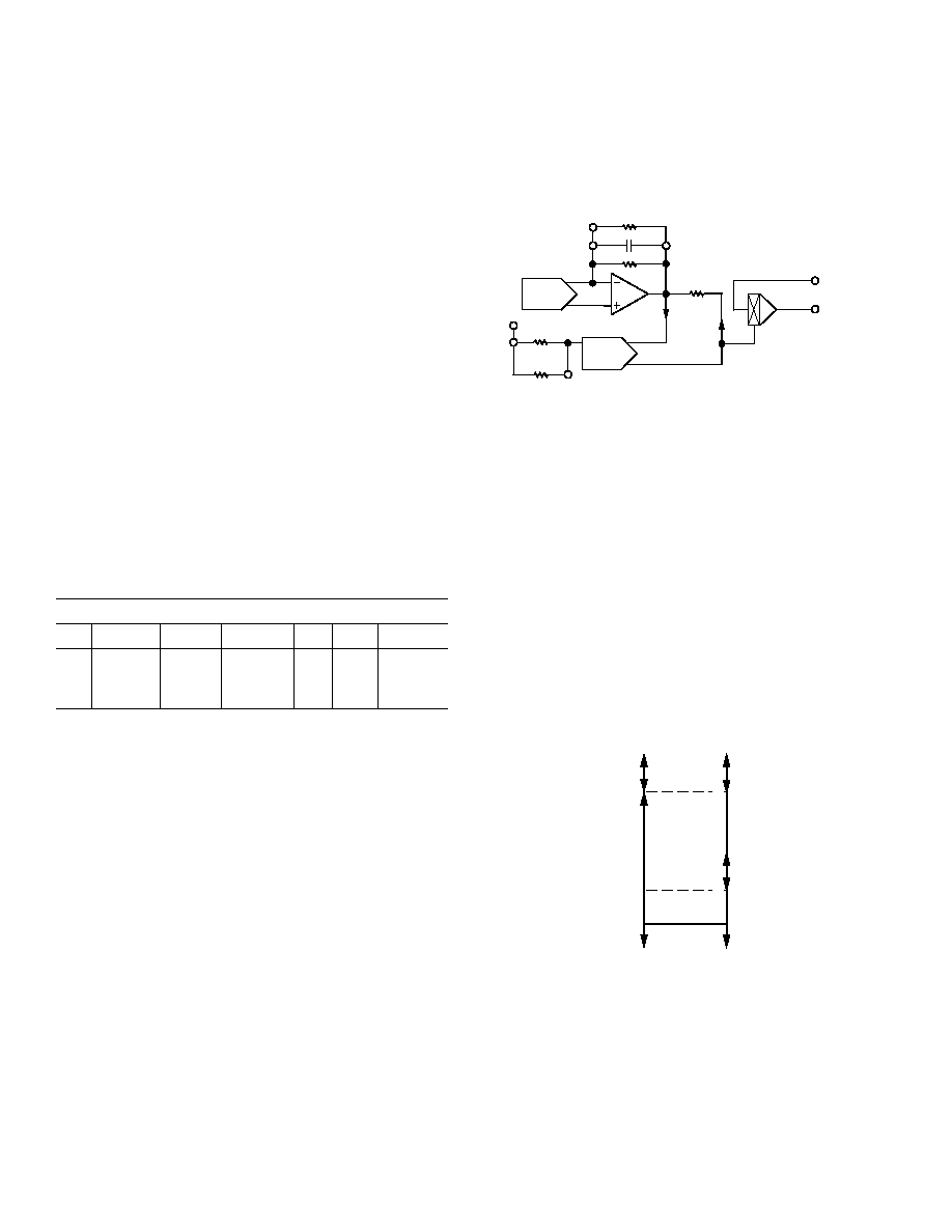
Figure 8. VCA Control Scheme
Control Range and Channel Tracking
Each channel VCA is controlled by its own DAC’s output, plus
the control signal from the master DAC. This is shown in Figure 8.
Channel DACs are configured to increase the gain of the VCA in
1 dB steps from 0 dB to 31 dB. Thus, the midpoint (15, or 16 if
preferred) should be chosen as the center setting of the electronic
balance controls. Since the master DAC feeds all summation
nodes, the attenuation of all VCAs simultaneously changes from
0 dB to the noise floor.
Maximum attenuation of all channels occurs when the master is
set to –127 dB attenuation, and the channel is set to 0 dB gain.
Minimum attenuation of all channels occurs when the master is
set at 0 dB, and the channel is set to 31 dB.
Once the channel-to-channel balance has been set, the master
may be changed without changing the balance. This is shown in
Figure 9.
+31
+16
0
–16
–32
–48
–64
–80
–96
–112
–128
0 0 0 0 0
1 1 1 1 1
0 0 0 0 0
1 1 1 1 1
CHANNEL
GAIN
CHANNEL
GAIN
CHANNEL
GAIN
MASTER
ATTENUATION
+31
+16
0
+31
+16
0
NOISE FLOOR
0 0 0 0 0 0
NET GAIN/ATTEN
1 1 1 1 1 1
Figure 9. Practical Control Range
Master/Channel Step Sizes
The details of the DAC control of the channel VCAs is depicted
in Figure 8. A 7-bit current output DAC and an op amp convert
the digitally commanded master control level to an analog voltage.
A capacitor across the feedback resistor limits the rate of change
at the output to prevent clicking. A 5-bit DAC converts the digi-
tally commanded channel control level to a voltage via a resistor R.
These two control signals sum in resistor R and are fed to the
channel VCA. Although we present the attenuation and gain as
two separate items, in fact, the VCA can be operated smoothly
相关PDF资料 |
PDF描述 |
|---|---|
| MS27473T18A32PB | CONN PLUG 32POS STRAIGHT W/PINS |
| VE-BWR-MY | CONVERTER MOD DC/DC 7.5V 50W |
| EN3P15F26SX | CONN RCPT 15POS FEMALE PANEL #26 |
| MS3100E28-6P | CONN RCPT 3POS WALL MNT W/PINS |
| PT00A-12-10P | CONN RCPT 10 POS WALL MNT W/PINS |
相关代理商/技术参数 |
参数描述 |
|---|---|
| SSM2160SZ-REEL | 功能描述:IC CTRLR DGTL VOL/CHAN 24SOIC RoHS:是 类别:集成电路 (IC) >> 线性 - 音频处理 系列:- 其它有关文件:STA321 View All Specifications 标准包装:1 系列:Sound Terminal™ 类型:音频处理器 应用:数字音频 安装类型:表面贴装 封装/外壳:64-LQFP 裸露焊盘 供应商设备封装:64-LQFP EP(10x10) 包装:Digi-Reel® 其它名称:497-11050-6 |
| SSM2161 | 制造商:AD 制造商全称:Analog Devices 功能描述:6- and 4-Channel, Serial Input Master/Balance Volume Controls |
| SSM2161N | 制造商:未知厂家 制造商全称:未知厂家 功能描述:Tone/Volume/Balance Control |
| SSM2161P | 制造商:AD 制造商全称:Analog Devices 功能描述:6- and 4-Channel, Serial Input Master/Balance Volume Controls |
| SSM2161R | 制造商:未知厂家 制造商全称:未知厂家 功能描述:Tone/Volume/Balance Control |
发布紧急采购,3分钟左右您将得到回复。