- 您现在的位置:买卖IC网 > PDF目录10951 > SSM2604CPZ-REEL7 (Analog Devices Inc)IC AUDIO CODEC LP 20-LFCSP PDF资料下载
参数资料
| 型号: | SSM2604CPZ-REEL7 |
| 厂商: | Analog Devices Inc |
| 文件页数: | 4/28页 |
| 文件大小: | 0K |
| 描述: | IC AUDIO CODEC LP 20-LFCSP |
| 标准包装: | 1 |
| 类型: | 立体声音频 |
| 数据接口: | 串行 |
| 分辨率(位): | 24 b |
| ADC / DAC 数量: | 2 / 2 |
| 三角积分调变: | 无 |
| S/N 比,标准 ADC / DAC (db): | 90 / 100 |
| 电压 - 电源,模拟: | 1.8 V ~ 3.6 V |
| 电压 - 电源,数字: | 1.5 V ~ 3.6 V |
| 工作温度: | -40°C ~ 85°C |
| 安装类型: | 表面贴装 |
| 封装/外壳: | 20-VFQFN 裸露焊盘,CSP |
| 供应商设备封装: | 20-LFCSP-VQ |
| 包装: | 标准包装 |
| 其它名称: | SSM2604CPZ-REEL7DKR |
第1页第2页第3页当前第4页第5页第6页第7页第8页第9页第10页第11页第12页第13页第14页第15页第16页第17页第18页第19页第20页第21页第22页第23页第24页第25页第26页第27页第28页
SSM2604
Data Sheet
Rev. A | Page 12 of 28
ANALOG INTERFACE
Signal Chain
The SSM2604 includes stereo single-ended line inputs to the
on-board ADC. In addition, the line inputs can be routed and
mixed directly to the output terminals via the BYPASS bit
(Register R4, Bit D3). The SSM2604 also includes line outputs
from the on-board DAC.
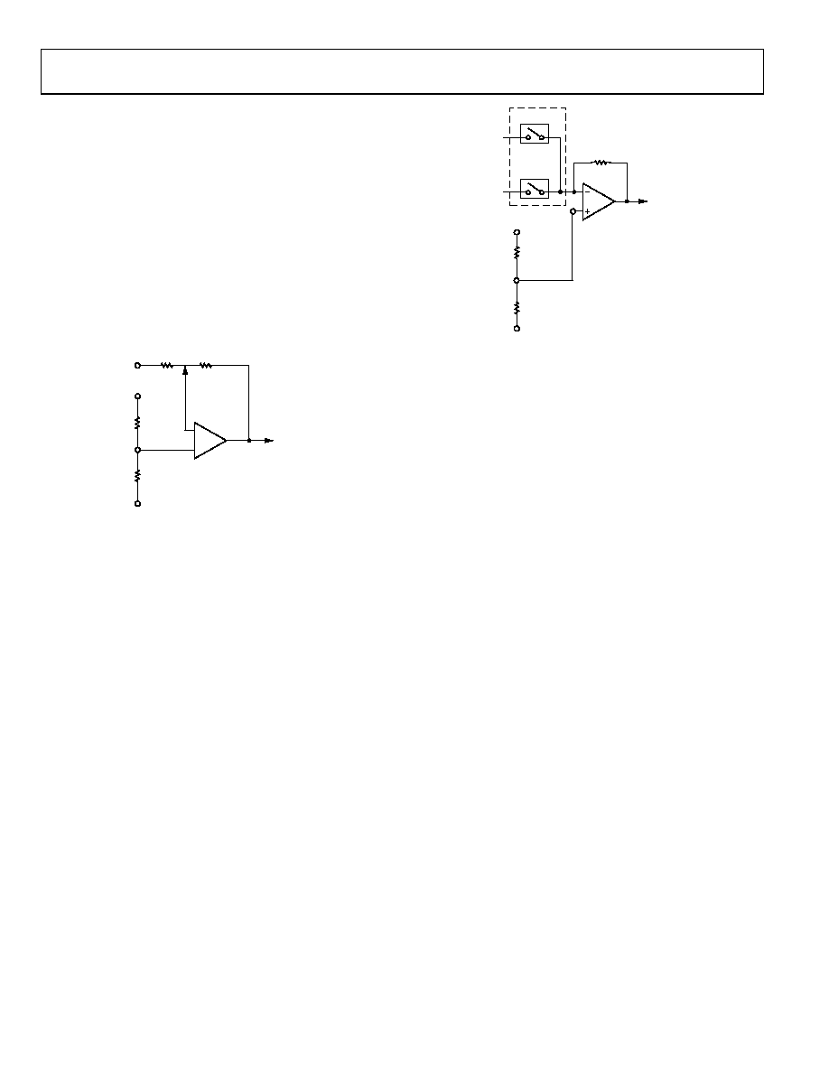
Stereo Line Inputs
The SSM2604 contains a set of single-ended stereo line inputs
(RLINEIN and LLINEIN) that are internally biased to VMID
by way of a voltage divider between AVDD and AGND. The
line input signal can be connected to the internal ADC and, if
desired, routed directly to the outputs via the bypass path by
using the BYPASS bit (Register R4, Bit D3).
ADC
OR
BYPASS
LINEIN
AVDD
VMID
AGND
+
–
06
97
8-
0
31
Figure 17. Line Input to ADC
The line input volume can be adjusted from 34.5 dB to +33 dB
in steps of +1.5 dB by setting the LINVOL (Register R0, Bit D0
to Bit D5) and RINVOL (Register R1, Bit D0 to Bit D5) bits.
Volume control, by default, is independently adjustable on
both right and left line inputs. However, the LRINBOTH or
RLINBOTH bit, if selected, simultaneously loads both sets of
volume control with the same value. The user can also set the
LINMUTE (Register R0, Bit D7) and RINMUTE (Register R1,
Bit D7) bits to mute the line input signal to the ADC.
Note that when sourcing audio data from line inputs, the maxi-
mum full-scale input of the ADC is 1.0 V rms when AVDD = 3.3 V.
Do not source any input voltage larger than full scale to avoid
overloading the ADC, which causes distortion of sound and
deterioration of audio quality. For best sound quality in line
inputs, gain should be carefully configured so that the ADC
receives a signal equal to its full scale. This maximizes the
signal-to-noise ratio for best total audio quality.
Bypass Path to Output
The line inputs can be routed and mixed directly to the output
terminals via the BYPASS (Register R4, Bit D3) software control
register selection. The analog input signal is routed directly to
the output terminals and is not digitally converted. The bypass
signal at the output mixer is the same level as the output of the
PGA associated with each line input.
Line Outputs
The DAC outputs and the line inputs (the bypass path) are
summed at an output mixer.
LINE OUTPUT
AVDD
VMID
AGND
BYPASS
DACSEL
LINE
INPUT
DAC
OUTPUT
06
97
8-
0
33
Figure 18. Output Signal Chain
The maximum output level of the line outputs is 1.0 V rms
when AVDD and HPVDD = 3.3 V. To suppress audible pops
and clicks, the line outputs are held at the VMID dc voltage
level when the device is set to standby mode.
The stereo line outputs of the SSM2604, the LOUT and
ROUT pins, are able to drive a load impedance of 10 kΩ and
50 pF. The line output signal levels are not adjustable at the
output mixer, having a fixed gain of 0 dB.
DIGITAL AUDIO INTERFACE
The digital audio input can support the following four
digital audio communication protocols: right-justified mode,
left-justified mode, I2S mode, and digital signal processor
(DSP) mode.
The mode selection is performed by writing to the FORMAT
bits of the digital audio interface register (Register R7, Bit D1
and Bit D0). All modes are MSB first and operate with data of
16 to 32 bits.
Recording Mode
On the RECDAT output pin, the digital audio interface can
send digital audio data for recording mode operation. The
digital audio interface outputs the processed internal ADC
digital filter data onto the RECDAT output. The digital audio
data stream on RECDAT comprises left- and right-channel
audio data that is time domain multiplexed.
The RECLRC is the digital audio frame clock signal that
separates left- and right-channel data on the RECDAT lines.
The BCLK signal acts as the digital audio clock. Depending on
if the SSM2604 is in master or slave mode, the BCLK signal is
either an input or an output signal. During a recording opera-
tion, RECDAT and RECLRC must be synchronous to the BCLK
signal to avoid data corruption.
Playback Mode
On the PBDAT input pin, the digital audio interface can receive
digital audio data for playback mode operation. The digital audio
data stream on PBDAT comprises left- and right-channel audio
data that is time domain multiplexed. The PBLRC is the digital
相关PDF资料 |
PDF描述 |
|---|---|
| MCIMX357DVM5B | PROCESSOR MULTIMEDIA 400PBGA |
| VI-26W-IY-F3 | CONVERTER MOD DC/DC 5.5V 50W |
| VI-26V-IY-F4 | CONVERTER MOD DC/DC 5.8V 50W |
| MAX9867ETJ+ | IC STEREO AUD CODEC LP 32TQFN-EP |
| MCIMX357DVM5BR2 | IC MPU I.MX35 400MAPBGA |
相关代理商/技术参数 |
参数描述 |
|---|---|
| SSM2604-EVALZ | 功能描述:BOARD EVAL SSM2604 RoHS:是 类别:编程器,开发系统 >> 评估演示板和套件 系列:- 标准包装:1 系列:- 主要目的:电信,线路接口单元(LIU) 嵌入式:- 已用 IC / 零件:IDT82V2081 主要属性:T1/J1/E1 LIU 次要属性:- 已供物品:板,电源,线缆,CD 其它名称:82EBV2081 |
| SSM2605GY | 制造商:SSC 制造商全称:Silicon Standard Corp. 功能描述:P-CHANNEL ENHANCEMENT MODE POWER MOSFET |
| SSM26PT | 制造商:CHENMKO 制造商全称:Chenmko Enterprise Co. Ltd. 功能描述:SCHOTTKY BARRIER RECTIFIER |
| SSM2761P-A | 制造商:SSC 制造商全称:Silicon Standard Corp. 功能描述:N-CHANNEL ENHANCEMENT MODE POWER MOSFET |
| SSM27APT | 制造商:CHENMKO 制造商全称:Chenmko Enterprise Co. Ltd. 功能描述:SCHOTTKY BARRIER RECTIFIER |
发布紧急采购,3分钟左右您将得到回复。